CERN/LHCC 2001-0011 31 May 2001cern.ch/lhcb-vd/TDR/velo_tdr.pdfCERN/LHCC 2001-0011 LHCb TDR 5 31 May...
97
O C L A T O R V E R T E X Technical Design Report CERN/LHCC 2001-0011 LHCb TDR 5 31 May 2001
Transcript of CERN/LHCC 2001-0011 31 May 2001cern.ch/lhcb-vd/TDR/velo_tdr.pdfCERN/LHCC 2001-0011 LHCb TDR 5 31 May...

OC
L
AT
ORV
ER
TEX
Technical Design Report
CERN/LHCC 2001-0011
LHCb TDR 5
31 May 2001

ii
iii
VELO TDR
The LHCb Collaboration1
Brasilian Research Center for Physics, CBPF, Rio de Janeiro, BrasilP.R. Barbosa Marinho, I. Bediaga, A. Franca Barbosa, J. Magnin, J. Marques de Miranda,A. Massaerri, A. Reis, R. Silva
University of Rio de Janeiro, UFRJ, Rio de Janeiro, BrasilS. Amato, P. Colrain, T. da Silva, J.R.T. de Mello Neto, L. de Paula, M. Gandelman,J.H. Lopes, B. Marechal, D. Moraes, E. Polycarpo
University of Clermont-Ferrand II, Clermont-Ferrand, FranceZ. Ajaltouni, G. Bohner, V. Breton, R. Cornat, O. Deschamps, A. Falvard1), P. Henrard,J. Lecoq, P. Perret, C. Rimbault, C. Trouilleau, A. Ziad
CPPM Marseille, Aix University-Marseille II, Marseille, FranceE. Aslanides, J.P. Cachemiche, R. Le Gac, O. Leroy, P.L. Liotard, M. Menouni, R. Potheau,A. Tsaregorodtsev, B. Viaud
University of Paris-Sud, LAL Orsay, Orsay, FranceG. Barrand, C. Beigbeder-Beau, D. Breton, T. Caceres, O. Callot, Ph. Cros, B. D'Almagne,B. Delcourt, F. Fulda Quenzer, A. Jacholkowska1), B. Jean- Marie, J. Lefrancois, F. Machefert,V. Tocut, K. Truong, I. Videau
Technical University of Dresden, Dresden, GermanyR. Schwierz, B. Spaan
Max-Planck-Institute for Nuclear Physics, Heidelberg, GermanyC. Bauer, D. Baumeister, N. Bulian, H.P. Fuchs, T. Glebe, W. Hofmann, K.T. Knop e,S. Lochner, M. Schmelling, B. Schwingenheuer, F. Sciacca, E. Sexauer2), U. Trunk
Physics Institute, University of Heidelberg, Heidelberg, GermanyS. Bachmann, P. Bock, H. Deppe, F. Eisele, M. Feuerstack-Raible, S. Henneberger, P. Igo-Kemenes, R. Rusnyak, U. Stange, M. Walter, D. Wiedner, U. Uwer
Kirchho Institute for Physics, University of Heidelberg, Heidelberg, GermanyV. Lindenstruth, R. Richter, M.W. Schulz, A. Walsch
Laboratori Nazionali dell' INFN, Frascati, ItalyG. Bencivenni, C. Bloise, F. Bossi, P. Campana, G. Capon, P. DeSimone, C. Forti,M.A. Franceschi, F. Murtas, L. Passalacqua, V. Patera(1), A. Sciubba(1)(1)also at Dipartimento di Energetica, University of Rome, \La Sapienza"
University of Bologna and INFN, Bologna, ItalyM. Bargiotti, A. Bertin, M. Bruschi, M. Capponi, I. D'Antone, S. de Castro, P. Faccioli,
1This list includes additional colleagues who made particular contributions to the work presented in this TDR
iv
L. Fabbri, D. Galli, B. Giacobbe, U. Marconi, I. Massa, M. Piccinini, M. Poli, N. Semprini-Cesari, R. Spighi, V. Vagnoni, S. Vecchi, M. Villa, A. Vitale, A. Zoccoli
University of Cagliari and INFN, Cagliari, ItalyA. Cardini, M. Caria, A. Lai, D. Pinci, B. Saitta(1)(1) also at CERN
University of Ferrara and INFN, Ferrara, ItalyV. Carassiti, A. Cotta Ramusino, P. Dalpiaz, A. Gianoli, M. Martini, F. Petrucci, M. Savrie
University of Florence and INFN, Florence, ItalyA. Bizzeti, M. Calvetti, G. Collazuol, G. Passaleva, M. Veltri
University of Genoa and INFN, Genoa, ItalyS. Cuneo, F. Fontanelli, V. Gracco, P. Musico, A. Petrolini, M. Sannino
University of Milano-Bicocca and INFN, Milano, ItalyM. Alemi, T. Bellunato(1), M. Calvi, C. Matteuzzi, M. Musy, P. Negri, M. Paganoni(1) also at CERN
University of Rome, \La Sapienza" and INFN, Rome, ItalyG. Auriemma(1), V. Bocci, C. Bosio, D. Fidanza(1), A. Frenkel, K. Harrison, G. Martellotti,S. Martinez, G. Penso, R. Santacesaria, C. Satriano(1), A. Satta(1) also at University of Basilicata, Potenza, Italy
University of Rome, \Tor Vergata" and INFN, Rome, ItalyG. Carboni, D. Domenici, G. Ganis, R. Messi, L. Pacciani, L. Paoluzi, E. Santovetti
NIKHEF, The NetherlandsG. van Apeldoorn(1,3), N. van Bakel(1,2), T.S. Bauer(1,4), M. van Beuzekom(1), H. BoerRookhuizen(1), J. van den Brand(1,2), H.J. Bulten(1,2), M. Doets(1), R. van der Eijk(1),I. Gouz(1,5), P. de Groen(1), V. Gromov(1), R. Hierck(1), L. Hommels(1), E. Jans(1),L. Jansen(1), A.P. Kaan(1), T. Ketel(1,2), S. Klous (1,2), B. Koene(1), M. Kraan(1),F. Kroes(1), J. Kuijt(1), M. Merk(1), F. Mul(2), M. Needham(1), H. Schuijlenburg(1),T. Sluijk(1), J. van Tilburg(1), J. Verkooyen(1), H. de Vries(1), L. Wiggers(1), N. Zaitsev(1,3)3),M. Zupan(1)(1) Foundation of Fundamental Research of Matter in the Netherlands,(2) Free University Amsterdam,(3) University of Amsterdam,(4) University of Utrecht,(5) on leave from Protvino
Institute of High Energy Physics, Beijing, P.R.C.C. Gao, C. Jiang, H. Sun, Z. Zhu
v
Research Centre of High Energy Physics, Tsinghua University, Beijing, P.R.C.M. Bisset, J.P. Cheng, Y.G. Cui, Y. Gao, H.J. He, Y.P. Kuang, Y.J. Li, Q. Li, Y. Liao, J.P. Ni,B.B. Shao,J.J. Su, Y.R. Tian, Q. Wang, Q.S. Yan
Institute for Nuclear Physics and University of Mining and Metalurgy, Krakow,PolandE. Banas, J. Blocki, K. Galuszka, L. Hajduk, P. Jalocha, P. Kapusta, B. Kisielewski,W. Kucewicz, T. Lesiak, J. Michalowski, B. Muryn, Z. Natkaniec, W. Ostrowicz, G. Polok,E. Rulikowska-Zarebska, M. Stodulski, M. Witek, P. Zychowski
Soltan Institute for Nuclear Physics, Warsaw, PolandM. Adamus, A. Chlopik, Z. Guzik, A. Nawrot, M. Szczekowski
Horia Hulubei-National Institute for Physics and Nuclear Engineering (IFIN-HH), Bucharest-Magurele, RomaniaD.V. Anghel4), C. Coca, A. Cimpean, G. Giolu, C. Magureanu, S. Popescu, T. Preda,A.M. Rosca(1), V.L. Rusu5)
(1) also at Humbolt University, Berlin
Institute for Nuclear Research (INR), Moscow, RussiaV. Bolotov, S. Filippov, J. Gavrilov, E. Guschin, V. Kloubov, L. Kravchuk, S. Laptev,V. Laptev, V. Postoev, A. Sadovski, I. Semeniouk
Institute of Theoretical and Experimental Physics (ITEP), Moscow, RussiaS. Barsuk, I. Belyaev, A. Golutvin, O. Gouchtchine, V. Kiritchenko, G. Kostina, N. Levitski,A. Morozov, P. Pakhlov, D. Roussinov, V. Rusinov, S. Semenov, A. Soldatov, E. Tarkovski
Budker Institute for Nuclear Physics (INP), Novosibirsk, RussiaK. Beloborodov, A. Bondar, A. Bozhenok, A. Buzulutskov, S. Eidelman, V. Golubev,S. Oreshkin, A. Poluektov, S. Serednyakov, L. Shekhtman, B. Shwartz, Z. Silagadze, A. Sokolov,A. Vasiljev
Institute for High Energy Physics (IHEP-Serpukhov), Protvino, RussiaL.A. Afanassieva, I.V. Ajinenko, K. Beloous, V. Brekhovskikh, S. Denissov, A.V. Dorokhov,R.I. Dzhelyadin, A. Kobelev, A.K. Konoplyannikov, A.K. Likhoded, V.D. Matveev, V. Novikov,V.F. Obraztsov, A.P. Ostankov, V.I. Rykalin, V.K. Semenov, M.M. Shapkin, N. Smirnov,A. Sokolov, M.M. Soldatov, V.V. Talanov, O.P. Yushchenko
Petersburg Nuclear Physics Institute, Gatchina, St.Petersburg, RussiaB. Botchine, S. Guetz, V. Lazarev, N. Saguidova, E. Spiridenkov, A. Vorobyov, An. Vorobyov
University of Barcelona, Barcelona, SpainR. Ballabriga(1), S. Ferragut, Ll. Garrido, D. Gascon, S. Luengo(1), R. Miquel6), D. Peralta,M. Rosello(1), X. Vilasis(1)(1) also at departament d'Engineria Electronica La Salle, Universitat Ramon Llull, Barcelona
University of Santiago de Compostela, Santiago de Compostela, SpainB. Adeva, P. Conde, F. Gomez, J.A. Hernando, A. Iglesias, A. Lopez-Aguera, A. Pazos, M. Plo,
vi
J.M. Rodriguez, J.J. Saborido, M.J. Tobar
University of Lausanne, Lausanne, SwitzerlandP. Bartalini, A. Bay, B. Carron, C. Currat, O. Dormond, F. Durrenmatt, Y. Ermoline, R. Frei,G. Gagliardi, G. Haefeli, J.P. Hertig, P. Koppenburg, T. Nakada(1), J.P. Perroud, F. Ronga,O. Schneider, L. Studer, M. Tareb, M.T. Tran(1) also at CERN, on leave from PSI Villigen
University of Zurich, Zurich, SwitzerlandR. Bernet, E. Holzschuh, P. Sievers, O. Steinkamp, U. Straumann, D. Wyler, M. Ziegler
Institute of Physics and Technologies, Kharkiv, UkraineS. Maznichenko, O. Omelaenko, Yu. Ranyuk
Institute for Nuclear Research, Kiev, UkraineV. Aushev, V. Kiva, I. Kolomiets, Yu. Pavlenko, V. Pugatch, Yu. Vasiliev, V. Zerkin
University of Bristol, Bristol, U.K.N.H. Brook, J.E. Cole, R.D. Head, A. Phillips, F.F. Wilson
University of Cambridge, Cambridge, U.K.K. George, V. Gibson, C.R. Jones, S.G. Katvars, C. Shepherd-Themistocleous, C.P. Ward,S.A. Wotton
Rutherford Appleton Laboratory, Chilton, U.K.C.A.J. Brew, C.J. Densham, S. Easo, B. Franek, J.G.V. Guy, R.N.J. Halsall, J.A. Lidbury,J.V. Morris, A. Papanestis, G.N. Patrick, F.J.P. Soler, S.A. Temple, M.L. Woodward
University of Edinburgh, Edinburgh, U.K.S. Eisenhardt, A. Khan, F. Muheim, S. Playfer, A. Walker
University of Glasgow, Glasgow, U.K.A.J. Flavell, A. Halley, V. O'Shea, F.J.P. Soler
University of Liverpool, Liverpool, U.K.S. Biagi, T. Bowcock, J. Carroll, R. Gamet, G. Gasse, M. McCubbin, C. Parkes, G. Patel,J. Palacios, U. Parzefall, J. Phillips, P. Sutclie, P. Turner, V. Wright
Imperial College, London, U.K.G.J. Barber, D. Clark, P. Dauncey, A. Duane, M. Girone(1), J. Hassard, R. Hill, M.J. John7),D.R. Price, P. Savage, B. Simmons, L. Toudup, D. Websdale(1) also at CERN
University of Oxford, Oxford, U.KM. Adinol, G. Damerell, J. Bibby, M.J. Charles, N. Harnew, F. Harris, I. McArthur,J. Rademacker, N.J. Smale, S. Topp-Jorgensen, G. Wilkinson
vii
CERN, Geneva, SwitzerlandF. Anghinol, F. Bal, M. Benayoun(1), W. Bonivento(2), A. Braem, J. Buytaert, M. Campbell,A. Cass, M. Cattaneo, E. Chesi, J. Christiansen, R. Chytracek8), J. Closier, P. Collins,G. Corti, C. D'Ambrosio, H. Dijkstra, J.P. Dufey, M. Elsing, M. Ferro-Luzzi, F. Fiedler,W. Flegel, F. Formenti, R. Forty, M. Frank, C. Frei, I. Garcia Alfonso, C. Gaspar, G. GraciaAbril, T. Gys, F. Hahn, S. Haider, J. Harvey, B. Hay9), E. van Herwijnen, H.J. Hilke,G. von Holtey, D. Hutchroft, R. Jacobsson, P. Jarron, C. Joram, B. Jost, A. Kashchuk(3),I. Korolko(4), D. Lacarrere, M. Laub, M. Letheren, J.F. Libby, R. Lindner, M. Losasso,P. Mato Vila, H. Muller, N. Neufeld, J. Ocariz10), S. Ponce, F. Ranjard, W. Riegler, F. Rohner,T. Ruf, S. Saladino11), S. Schmeling, B. Schmidt, T. Schneider, A. Schopper, W. Snoeys,V. Souvorov(3), W. Tejessy, F. Teubert, J. Toledo Alarcon, O. Ullaland, A. Valassi, P. VazquezRegueiro, F. Vinci do Santos(5), P. Wertelaers, A. Wright12), K. Wyllie
(1) on leave from Universite de Paris VI et VII (LPNHE), Paris(2) on leave from INFN Cagliari, Cagliari(3) on leave from Petersburg Nuclear Physics Institute, Gatchina, St.Petersburg(4) on leave from ITEP, Moscow(5) on leave from UFRJ, Rio de Janeiro
1) now at Groupe d'Astroparticules de Montpellier (GAM), Montpellier, France2) now at Dialog Semiconductor, Kirchheim-Nabern, Germany3) now at Fortis Bank, Netherlands4) now at Oslo University, Oslo, Norway5) now at Pennsylvania University, Philadelphia, USA6) now at LBNL, Berkeley, USA7) now at College de France, Paris, France8) now at IT Division, CERN, Geneva, Switzerland9) now at SWX Swiss Exchange, Geneve, Switzerland10) now at Universite de Paris VI et VII (LPNHE), Paris, France12) now at Prevessin, France11) now at Lancaster University, Lancaster, UK

viii
Acknowledgments
The LHCb Collaboration is greatly indebted to all the technical and administrative sta fortheir important contributions to the design, testing and prototype activities. We are gratefulfor their dedicated work and are aware that the successful construction and commissioning ofthe LHCb experiment will also in future depend on their skills and commitment. The helpprovided by the CERN Accelerator Physics and LHC vacuum groups in the design of the VELOvacuum vessel is greatly appreciated. We also like to thank L. Gatignon and the sta of theCERN accelerator complex for their support during the test-beam periods. It is a pleasure toacknowledge the contribution of: E. Chesi, R. de Oliveira, A. Gandi, A. Honma, J.R. Moser,K. Muhlemann and A. Teixeira.

Contents
Acknowledgments . . . . . . . . . . . . . . . . . . . . . . . . . . . . . . . viii
1 Introduction 1
1.1 Physics requirements . . . . . . . . . . . . . . . . . . . . . . . . . . . . . . . . . . 1
1.2 VELO system overview . . . . . . . . . . . . . . . . . . . . . . . . . . . . . . . . 2
1.2.1 Constraints . . . . . . . . . . . . . . . . . . . . . . . . . . . . . . . . . . . 2
1.2.2 Overall dimensions . . . . . . . . . . . . . . . . . . . . . . . . . . . . . . . 3
1.2.3 Sensors . . . . . . . . . . . . . . . . . . . . . . . . . . . . . . . . . . . . . 5
1.2.4 Readout electronics . . . . . . . . . . . . . . . . . . . . . . . . . . . . . . 6
1.2.5 Detector cooling system . . . . . . . . . . . . . . . . . . . . . . . . . . . . 7
1.2.6 Integration with LHC . . . . . . . . . . . . . . . . . . . . . . . . . . . . . 7
1.2.7 Alignment . . . . . . . . . . . . . . . . . . . . . . . . . . . . . . . . . . . . 8
1.2.8 Material budget . . . . . . . . . . . . . . . . . . . . . . . . . . . . . . . . 9
1.2.9 Detector resolution . . . . . . . . . . . . . . . . . . . . . . . . . . . . . . . 9
1.3 Evolution since the Technical Proposal . . . . . . . . . . . . . . . . . . . . . . . . 9
1.4 Structure of this document . . . . . . . . . . . . . . . . . . . . . . . . . . . . . . 10
2 Summary of R&D and test of prototypes 11
2.1 Silicon . . . . . . . . . . . . . . . . . . . . . . . . . . . . . . . . . . . . . . . . . . 11
2.1.1 Design parameters . . . . . . . . . . . . . . . . . . . . . . . . . . . . . . . 11
Thickness . . . . . . . . . . . . . . . . . . . . . . . . . . . . . . . . . . . . 11
Segmentation . . . . . . . . . . . . . . . . . . . . . . . . . . . . . . . . . . 12
Oxygenation . . . . . . . . . . . . . . . . . . . . . . . . . . . . . . . . . . 13
Cryogenic operation . . . . . . . . . . . . . . . . . . . . . . . . . . . . . . 13
2.1.2 Prototype designs . . . . . . . . . . . . . . . . . . . . . . . . . . . . . . . 13
2.1.3 Prototype manufacture . . . . . . . . . . . . . . . . . . . . . . . . . . . . 14
2.1.4 Prototype tests . . . . . . . . . . . . . . . . . . . . . . . . . . . . . . . . . 15
2.1.5 Laboratory tests . . . . . . . . . . . . . . . . . . . . . . . . . . . . . . . . 16
PR01 Prototype . . . . . . . . . . . . . . . . . . . . . . . . . . . . . . . . 16
PR02 Prototype . . . . . . . . . . . . . . . . . . . . . . . . . . . . . . . . 16
2.1.6 Test-beam results on non-irradiated sensors . . . . . . . . . . . . . . . . . 17
Common mode and noise analysis . . . . . . . . . . . . . . . . . . . . . . 17
Track tting and alignment . . . . . . . . . . . . . . . . . . . . . . . . . . 18
Triggering . . . . . . . . . . . . . . . . . . . . . . . . . . . . . . . . . . . . 18
Resolution . . . . . . . . . . . . . . . . . . . . . . . . . . . . . . . . . . . . 18
SCT128A performance . . . . . . . . . . . . . . . . . . . . . . . . . . . . . 19
2.1.7 Irradiation procedures . . . . . . . . . . . . . . . . . . . . . . . . . . . . . 20
2.1.8 Test-beam results on irradiated sensors . . . . . . . . . . . . . . . . . . . 20
ix
x CONTENTS
DELPHI-ds prototype . . . . . . . . . . . . . . . . . . . . . . . . . . . . . 21
PR01 prototypes . . . . . . . . . . . . . . . . . . . . . . . . . . . . . . . . 21
PR02 prototype . . . . . . . . . . . . . . . . . . . . . . . . . . . . . . . . 22
2.1.9 Measurements with a laser . . . . . . . . . . . . . . . . . . . . . . . . . . 24
2.1.10 Summary . . . . . . . . . . . . . . . . . . . . . . . . . . . . . . . . . . . . 25
2.2 Hybrid . . . . . . . . . . . . . . . . . . . . . . . . . . . . . . . . . . . . . . . . . . 26
2.3 VELO modules . . . . . . . . . . . . . . . . . . . . . . . . . . . . . . . . . . . . . 27
2.4 Front-end electronics . . . . . . . . . . . . . . . . . . . . . . . . . . . . . . . . . . 29
2.4.1 Front-end chip . . . . . . . . . . . . . . . . . . . . . . . . . . . . . . . . . 29
The SCT128A and SCTA VELO chips . . . . . . . . . . . . . . . . . . . . 30
The Beetle chip . . . . . . . . . . . . . . . . . . . . . . . . . . . . . . . . . 30
2.4.2 L1 Electronics . . . . . . . . . . . . . . . . . . . . . . . . . . . . . . . . . 31
2.5 Mechanics, wake elds, cooling and vacuum . . . . . . . . . . . . . . . . . . . . . 34
2.5.1 Mechanical aspects of the secondary vacuum container . . . . . . . . . . . 34
2.5.2 The secondary vacuum container as a wake eld suppressor . . . . . . . . 35
2.5.3 Protection of the secondary vacuum container . . . . . . . . . . . . . . . . 38
2.5.4 Proof-of-principle of the CO2 cooling system . . . . . . . . . . . . . . . . 38
3 Technical design 41
3.1 Sensors . . . . . . . . . . . . . . . . . . . . . . . . . . . . . . . . . . . . . . . . . 41
3.1.1 Operating conditions for the silicon sensors . . . . . . . . . . . . . . . . . 44
3.2 Modules . . . . . . . . . . . . . . . . . . . . . . . . . . . . . . . . . . . . . . . . . 45
3.3 Front-end electronics . . . . . . . . . . . . . . . . . . . . . . . . . . . . . . . . . . 46
3.3.1 System architecture . . . . . . . . . . . . . . . . . . . . . . . . . . . . . . 46
3.3.2 L0 Electronics . . . . . . . . . . . . . . . . . . . . . . . . . . . . . . . . . 46
Front-end chip . . . . . . . . . . . . . . . . . . . . . . . . . . . . . . . . . 46
The ECS interface . . . . . . . . . . . . . . . . . . . . . . . . . . . . . . . 49
Hybrid . . . . . . . . . . . . . . . . . . . . . . . . . . . . . . . . . . . . . . 50
3.3.3 L1 Electronics . . . . . . . . . . . . . . . . . . . . . . . . . . . . . . . . . 50
Repeater cards . . . . . . . . . . . . . . . . . . . . . . . . . . . . . . . . . 50
Analog data transmission . . . . . . . . . . . . . . . . . . . . . . . . . . . 50
Digitizer board . . . . . . . . . . . . . . . . . . . . . . . . . . . . . . . . . 50
3.3.4 Power supplies . . . . . . . . . . . . . . . . . . . . . . . . . . . . . . . . . 52
Low voltage modules . . . . . . . . . . . . . . . . . . . . . . . . . . . . . . 52
High voltage modules . . . . . . . . . . . . . . . . . . . . . . . . . . . . . 53
Crate controller module . . . . . . . . . . . . . . . . . . . . . . . . . . . . 53
Cables . . . . . . . . . . . . . . . . . . . . . . . . . . . . . . . . . . . . . . 53
3.3.5 Grounding scheme . . . . . . . . . . . . . . . . . . . . . . . . . . . . . . . 53
3.4 Mechanics . . . . . . . . . . . . . . . . . . . . . . . . . . . . . . . . . . . . . . . . 54
3.4.1 Mechanical design . . . . . . . . . . . . . . . . . . . . . . . . . . . . . . . 55
3.5 Vacuum system . . . . . . . . . . . . . . . . . . . . . . . . . . . . . . . . . . . . . 58
3.5.1 Layout . . . . . . . . . . . . . . . . . . . . . . . . . . . . . . . . . . . . . . 58
3.5.2 Protection devices of the LHCb vacuum system . . . . . . . . . . . . . . . 61
3.5.3 LHCb vacuum: eects on LHC operation . . . . . . . . . . . . . . . . . . 61
3.5.4 Risk analysis . . . . . . . . . . . . . . . . . . . . . . . . . . . . . . . . . . 62
3.6 Cooling . . . . . . . . . . . . . . . . . . . . . . . . . . . . . . . . . . . . . . . . . 62
3.7 Material budget . . . . . . . . . . . . . . . . . . . . . . . . . . . . . . . . . . . . . 63
3.8 Alignment . . . . . . . . . . . . . . . . . . . . . . . . . . . . . . . . . . . . . . . . 64
CONTENTS xi
3.9 Safety aspects . . . . . . . . . . . . . . . . . . . . . . . . . . . . . . . . . . . . . . 66
4 Simulation results 674.1 Software and event samples . . . . . . . . . . . . . . . . . . . . . . . . . . . . . . 674.2 Optimization . . . . . . . . . . . . . . . . . . . . . . . . . . . . . . . . . . . . . . 67
4.2.1 Overall detector optimization . . . . . . . . . . . . . . . . . . . . . . . . . 674.2.2 Impact on L1 trigger . . . . . . . . . . . . . . . . . . . . . . . . . . . . . . 67
4.3 Particle uxes . . . . . . . . . . . . . . . . . . . . . . . . . . . . . . . . . . . . . . 684.4 Physics performance . . . . . . . . . . . . . . . . . . . . . . . . . . . . . . . . . . 69
4.4.1 Impact parameter resolution . . . . . . . . . . . . . . . . . . . . . . . . . 694.4.2 Primary vertex, decay length and time resolutions . . . . . . . . . . . . . 714.4.3 Invariant mass resolutions . . . . . . . . . . . . . . . . . . . . . . . . . . . 72
5 Project organization 735.1 Schedule . . . . . . . . . . . . . . . . . . . . . . . . . . . . . . . . . . . . . . . . . 73
5.1.1 Completion of design and prototyping . . . . . . . . . . . . . . . . . . . . 735.1.2 Construction . . . . . . . . . . . . . . . . . . . . . . . . . . . . . . . . . . 735.1.3 Installation and commissioning . . . . . . . . . . . . . . . . . . . . . . . . 75
5.2 Milestones . . . . . . . . . . . . . . . . . . . . . . . . . . . . . . . . . . . . . . . . 755.3 Costs . . . . . . . . . . . . . . . . . . . . . . . . . . . . . . . . . . . . . . . . . . . 755.4 Division of responsibilities . . . . . . . . . . . . . . . . . . . . . . . . . . . . . . . 79
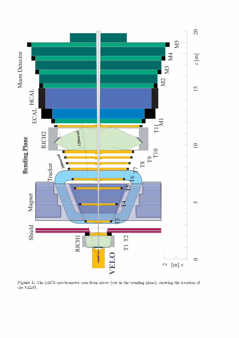
Figure 1: The LHCb spectrometer seen from above (cut in the bending plane), showing the location ofthe VELO.
1 Introduction
Vertex reconstruction is a fundamental re-quirement for the LHCb experiment. Dis-placed secondary vertices are a distinctive fea-ture of b-hadron decays. TheVErtex LOcator(VELO) has to provide precise measurementsof track coordinates close to the interaction re-gion. These are used to reconstruct produc-tion and decay vertices of beauty- and charm-hadrons, to provide an accurate measurementof their decay lifetimes, and to measure theimpact parameter of particles used to tag their avor. The VELO measurements are also a vi-tal input to the second level trigger (L1), whichenriches the b-decay content of the data.
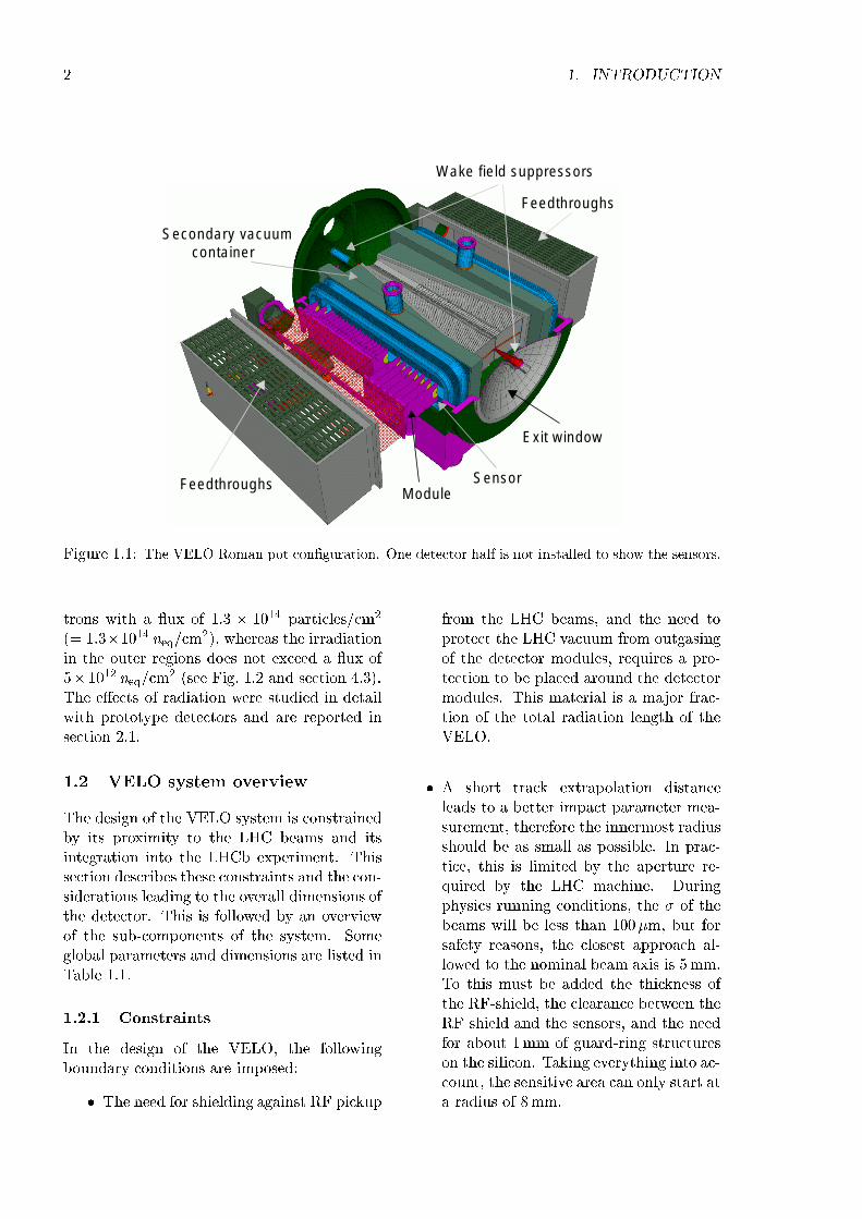
The VELO features a series of silicon sta-tions placed along the beam direction. Theyare placed at a radial distance from the beamwhich is smaller than the aperture required bythe LHC during injection and must thereforebe retractable. This is achieved by mountingthe detectors in a setup similar to Roman pots(Fig. 1.1). The placement of the VELO withinthe LHCb spectrometer can be seen in Fig. 1,which shows the top view of the LHCb spec-trometer. Details of the rest of the experimentcan be found in [1, 2]. In this introduction,the physics requirements are discussed, and anoverview is given of the VELO detector sys-tem. A brief discussion of the evolution sincethe Technical Proposal is then given, before anoutline of the rest of the document.
1.1 Physics requirements
The basic tasks of the LHCb VELO systemare the reconstruction of the position of theprimary vertex, the detection of tracks whichdo not originate from the primary vertex andthe reconstruction of b-hadron decay vertices.
The VELO has to cover completely the angularacceptance of the downstream detectors.
Special requirements emerge from the useof the VELO information in the L1 trigger.The L1 algorithm requires a fast and stand-alone three-dimensional pattern recognition todistinguish b-events from those minimum biasevents which are accepted by the rst level trig-ger (L0). B-hadrons that have all their decayproducts within the acceptance of the spec-trometer are typically produced with a polarangle below 200mrad. Hence, the projectionof the impact parameter of the decay productsto the primary vertex in the rz-plane is large,while in the plane perpendicular to the beam-axis (r) it is similar to that of tracks originat-ing from the primary vertex. The L1 triggerexploits this by rst reconstructing all tracksin the rz-projection, but reconstructing onlytracks in three dimensions which have a sig-nicant rz-impact parameter. Hence, the strippattern on the sensors has strips with constantradius for the rz-track reconstruction, com-bined with radial-strip sensors having a stereoangle of (10Æ20Æ) to allow the two projectionsto be combined.
The r-geometry has also the advantagethat it allows in a natural way to choose thesmallest strip pitch close to the beam axis,hence best hit resolution where it is needed,and larger strip pitches towards the outsideof the sensors. This minimizes the number ofreadout channels and results in a balanced oc-cupancy throughout the sensor.
The detectors have to operate in an ex-treme radiation environment which is stronglynon-uniform. The damage to silicon at themost irradiated area during one year of op-eration is equivalent to that of 1MeV neu-
1
2 1. INTRODUCTION
Secondary vacuum container
Wake field suppressors
Exit window
SensorModule
Feedthroughs
Feedthroughs
Figure 1.1: The VELO Roman pot conguration. One detector half is not installed to show the sensors.
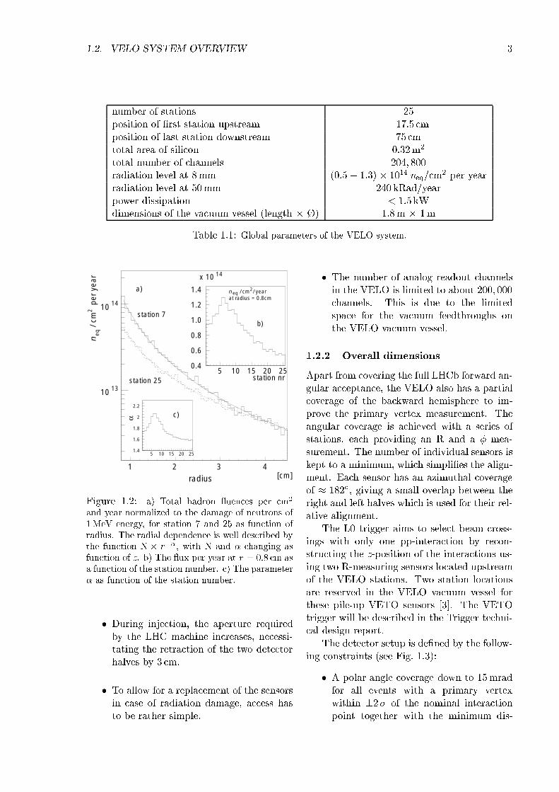
trons with a ux of 1:3 1014 particles/cm2
(= 1:31014 neq/cm2), whereas the irradiationin the outer regions does not exceed a ux of5 1012 neq/cm
2 (see Fig. 1.2 and section 4.3).The eects of radiation were studied in detailwith prototype detectors and are reported insection 2.1.
1.2 VELO system overview
The design of the VELO system is constrainedby its proximity to the LHC beams and itsintegration into the LHCb experiment. Thissection describes these constraints and the con-siderations leading to the overall dimensions ofthe detector. This is followed by an overviewof the sub-components of the system. Someglobal parameters and dimensions are listed inTable 1.1.
1.2.1 Constraints
In the design of the VELO, the followingboundary conditions are imposed:
The need for shielding against RF pickup
from the LHC beams, and the need toprotect the LHC vacuum from outgasingof the detector modules, requires a pro-tection to be placed around the detectormodules. This material is a major frac-tion of the total radiation length of theVELO.
A short track extrapolation distanceleads to a better impact parameter mea-surement, therefore the innermost radiusshould be as small as possible. In prac-tice, this is limited by the aperture re-quired by the LHC machine. Duringphysics running conditions, the of thebeams will be less than 100m, but forsafety reasons, the closest approach al-lowed to the nominal beam axis is 5mm.To this must be added the thickness ofthe RF-shield, the clearance between theRF shield and the sensors, and the needfor about 1mm of guard-ring structureson the silicon. Taking everything into ac-count, the sensitive area can only start ata radius of 8mm.
1.2. VELO SYSTEM OVERVIEW 3
number of stations 25position of rst station upstream 17:5 cmposition of last station downstream 75 cmtotal area of silicon 0:32m2
total number of channels 204; 800radiation level at 8mm (0:5 1:3) 1014 neq/cm
2 per yearradiation level at 50mm 240 kRad/yearpower dissipation < 1:5 kWdimensions of the vacuum vessel (length ) 1:8m 1m
Table 1.1: Global parameters of the VELO system.
1.4
1.6
1.8
2
2.2
5 10 15 20 25
α
10 13
10 14
1 2 3 4[cm]
c)
a)
station 7
station 25
radius
n
/ cm
pe
r ye
ar2
eq
0.4
0.6
0.8
1.0
1.2
1.4
x 10 14
5 10 15 20 25station nr
b)
n / cm / year at radius = 0.8cm
2eq
Figure 1.2: a) Total hadron uences per cm2
and year normalized to the damage of neutrons of1MeV energy, for station 7 and 25 as function ofradius. The radial dependence is well described bythe function N r, with N and changing asfunction of z. b) The ux per year at r = 0:8 cm asa function of the station number. c) The parameter as function of the station number.
During injection, the aperture requiredby the LHC machine increases, necessi-tating the retraction of the two detectorhalves by 3 cm.
To allow for a replacement of the sensorsin case of radiation damage, access hasto be rather simple.
The number of analog readout channelsin the VELO is limited to about 200; 000channels. This is due to the limitedspace for the vacuum feedthroughs onthe VELO vacuum vessel.
1.2.2 Overall dimensions
Apart from covering the full LHCb forward an-gular acceptance, the VELO also has a partialcoverage of the backward hemisphere to im-prove the primary vertex measurement. Theangular coverage is achieved with a series ofstations, each providing an R and a mea-surement. The number of individual sensors iskept to a minimum, which simplies the align-ment. Each sensor has an azimuthal coverageof 182Æ, giving a small overlap between theright and left halves which is used for their rel-ative alignment.
The L0 trigger aims to select beam cross-ings with only one pp-interaction by recon-structing the z-position of the interactions us-ing two R-measuring sensors located upstreamof the VELO stations. Two station locationsare reserved in the VELO vacuum vessel forthese pile-up VETO sensors [3]. The VETOtrigger will be described in the Trigger techni-cal design report.
The detector setup is dened by the follow-ing constraints (see Fig. 1.3):
A polar angle coverage down to 15mradfor all events with a primary vertexwithin 2 of the nominal interactionpoint together with the minimum dis-
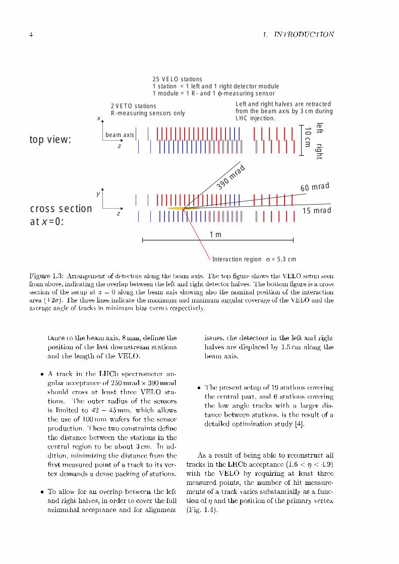
4 1. INTRODUCTION
1 m
10 cm
15 mrad
390 mrad
z
x
cross sectionat x =0:
top view:
z
y60 mrad
2 VETO stationsR-measuring sensors only
Interaction region σ = 5.3 cm
right
beam axis
Left and right halves are retractedfrom the beam axis by 3 cm duringLHC injection.
25 VELO stations1 station = 1 left and 1 right detector module1 module = 1 R- and 1 φ-measuring sensor
left
Figure 1.3: Arrangement of detectors along the beam axis. The top gure shows the VELO setup seenfrom above, indicating the overlap between the left and right detector halves. The bottom gure is a crosssection of the setup at x = 0 along the beam axis showing also the nominal position of the interactionarea (2). The three lines indicate the maximum and minimum angular coverage of the VELO and theaverage angle of tracks in minimum bias events respectively.
tance to the beam axis, 8mm, denes theposition of the last downstream stationsand the length of the VELO.
A track in the LHCb spectrometer an-gular acceptance of 250mrad 300mradshould cross at least three VELO sta-tions. The outer radius of the sensorsis limited to 42 45mm, which allowsthe use of 100mm wafers for the sensorproduction. These two constraints denethe distance between the stations in thecentral region to be about 3 cm. In ad-dition, minimizing the distance from therst measured point of a track to its ver-tex demands a dense packing of stations.
To allow for an overlap between the leftand right halves, in order to cover the fullazimuthal acceptance and for alignment
issues, the detectors in the left and righthalves are displaced by 1:5 cm along thebeam axis.
The present setup of 19 stations coveringthe central part, and 6 stations coveringthe low angle tracks with a larger dis-tance between stations, is the result of adetailed optimization study [4].
As a result of being able to reconstruct alltracks in the LHCb acceptance (1:6 < < 4:9)with the VELO by requiring at least threemeasured points, the number of hit measure-ments of a track varies substantially as a func-tion of and the position of the primary vertex(Fig. 1.4).
1.2. VELO SYSTEM OVERVIEW 5
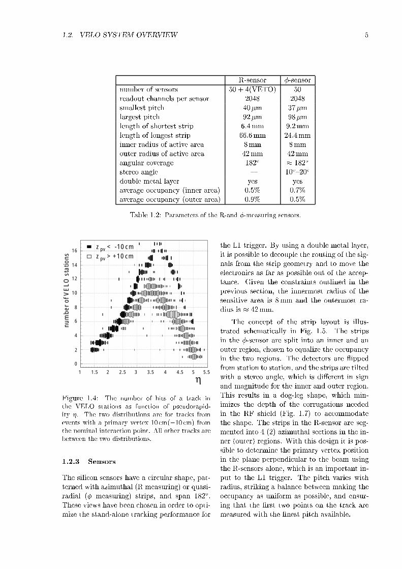
R-sensor -sensor
number of sensors 50 + 4(VETO) 50readout channels per sensor 2048 2048smallest pitch 40m 37mlargest pitch 92m 98mlength of shortest strip 6:4mm 9:2mmlength of longest strip 66:6mm 24:4mminner radius of active area 8mm 8mmouter radius of active area 42mm 42mmangular coverage 182Æ 182Æ
stereo angle 10Æ20Æ
double metal layer yes yesaverage occupancy (inner area) 0:5% 0:7%average occupancy (outer area) 0:9% 0:5%
Table 1.2: Parameters of the R-and -measuring sensors.
num
ber
of V
ELO
sta
tions
η
z < -10 cmpv
z > +10 cmpv
1 1.5 2 2.5 3 3.5 4 4.5 5 5.5
16
8
14
10
12
2
4
6
0
Figure 1.4: The number of hits of a track inthe VELO stations as function of pseudorapid-ity . The two distributions are for tracks fromevents with a primary vertex 10 cm(10 cm) fromthe nominal interaction point. All other tracks arebetween the two distributions.
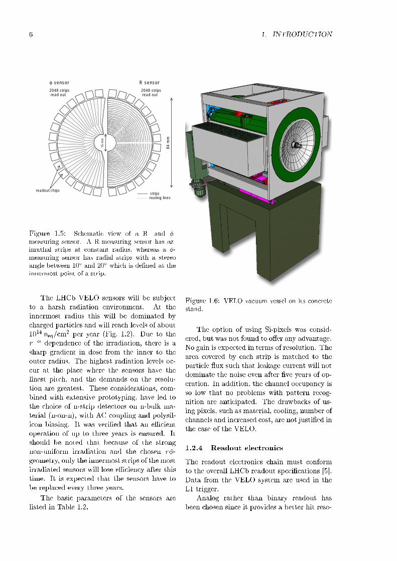
1.2.3 Sensors
The silicon sensors have a circular shape, pat-terned with azimuthal (R measuring) or quasi-radial ( measuring) strips, and span 182Æ.These views have been chosen in order to opti-mize the stand-alone tracking performance for
the L1 trigger. By using a double metal layer,it is possible to decouple the routing of the sig-nals from the strip geometry and to move theelectronics as far as possible out of the accep-tance. Given the constraints outlined in theprevious section, the innermost radius of thesensitive area is 8mm and the outermost ra-dius is 42mm.
The concept of the strip layout is illus-trated schematically in Fig. 1.5. The stripsin the -sensor are split into an inner and anouter region, chosen to equalize the occupancyin the two regions. The detectors are ippedfrom station to station, and the strips are tiltedwith a stereo angle, which is dierent in signand magnitude for the inner and outer region.This results in a dog-leg shape, which min-imizes the depth of the corrugations neededin the RF shield (Fig. 1.7) to accommodatethe shape. The strips in the R-sensor are seg-mented into 4 (2) azimuthal sections in the in-ner (outer) regions. With this design it is pos-sible to determine the primary vertex positionin the plane perpendicular to the beam usingthe R-sensors alone, which is an important in-put to the L1 trigger. The pitch varies withradius, striking a balance between making theoccupancy as uniform as possible, and ensur-ing that the rst two points on the track aremeasured with the nest pitch available.
6 1. INTRODUCTION
R sensor
stripsreadout chips
routing lines
φ sensor
84 m
m
16 m
m
2048 strips read out
2048 strips read out
Figure 1.5: Schematic view of a R- and -measuring sensor. A R-measuring sensor has az-imuthal strips at constant radius, whereas a -measuring sensor has radial strips with a stereoangle between 10Æ and 20Æ which is dened at theinnermost point of a strip.
The LHCb VELO sensors will be subjectto a harsh radiation environment. At theinnermost radius this will be dominated bycharged particles and will reach levels of about1014 neq/cm
2 per year (Fig. 1.2). Due to ther dependence of the irradiation, there is asharp gradient in dose from the inner to theouter radius. The highest radiation levels oc-cur at the place where the sensors have thenest pitch, and the demands on the resolu-tion are greatest. These considerations, com-bined with extensive prototyping, have led tothe choice of n-strip detectors on n-bulk ma-terial (n-on-n), with AC coupling and polysil-icon biasing. It was veried that an eÆcientoperation of up to three years is ensured. Itshould be noted that because of the strongnon-uniform irradiation and the chosen r-geometry, only the innermost strips of the mostirradiated sensors will lose eÆciency after thistime. It is expected that the sensors have tobe replaced every three years.
The basic parameters of the sensors arelisted in Table 1.2.
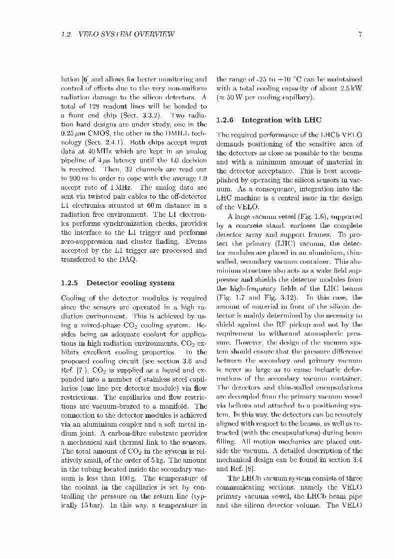
Figure 1.6: VELO vacuum vessel on its concretestand.
The option of using Si-pixels was consid-ered, but was not found to oer any advantage.No gain is expected in terms of resolution. Thearea covered by each strip is matched to theparticle ux such that leakage current will notdominate the noise even after ve years of op-eration. In addition, the channel occupancy isso low that no problems with pattern recog-nition are anticipated. The drawbacks of us-ing pixels, such as material, cooling, number ofchannels and increased cost, are not justied inthe case of the VELO.
1.2.4 Readout electronics
The readout electronics chain must conformto the overall LHCb readout specications [5].Data from the VELO system are used in theL1 trigger.
Analog rather than binary readout hasbeen chosen since it provides a better hit reso-
1.2. VELO SYSTEM OVERVIEW 7
lution [6] and allows for better monitoring andcontrol of eects due to the very non-uniformradiation damage to the silicon detectors. Atotal of 128 readout lines will be bonded toa front end chip (Sect. 3.3.2). Two radia-tion hard designs are under study, one in the0:25m CMOS, the other in the DMILL tech-nology (Sect. 2.4.1). Both chips accept inputdata at 40MHz which are kept in an analogpipeline of 4s latency until the L0 decisionis received. Then, 32 channels are read outin 900 ns in order to cope with the average L0accept rate of 1MHz. The analog data aresent via twisted pair cables to the o-detectorL1 electronics situated at 60m distance in aradiation free environment. The L1 electron-ics performs synchronization checks, providesthe interface to the L1 trigger and performszero-suppression and cluster nding. Eventsaccepted by the L1 trigger are processed andtransferred to the DAQ.
1.2.5 Detector cooling system
Cooling of the detector modules is requiredsince the sensors are operated in a high ra-diation environment. This is achieved by us-ing a mixed-phase CO2 cooling system. Be-sides being an adequate coolant for applica-tions in high radiation environments, CO2 ex-hibits excellent cooling properties. In theproposed cooling circuit (see section 3.6 andRef. [7]), CO2 is supplied as a liquid and ex-panded into a number of stainless steel capil-laries (one line per detector module) via owrestrictions. The capillaries and ow restric-tions are vacuum-brazed to a manifold. Theconnection to the detector modules is achievedvia an aluminium coupler and a soft metal in-dium joint. A carbon-bre substrate providesa mechanical and thermal link to the sensors.The total amount of CO2 in the system is rel-atively small, of the order of 5 kg. The amountin the tubing located inside the secondary vac-uum is less than 100 g. The temperature ofthe coolant in the capillaries is set by con-trolling the pressure on the return line (typ-ically 15 bar). In this way, a temperature in
the range of -25 to +10 ÆC can be maintainedwith a total cooling capacity of about 2:5 kW( 50W per cooling capillary).
1.2.6 Integration with LHC
The required performance of the LHCb VELOdemands positioning of the sensitive area ofthe detectors as close as possible to the beamsand with a minimum amount of material inthe detector acceptance. This is best accom-plished by operating the silicon sensors in vac-uum. As a consequence, integration into theLHC machine is a central issue in the designof the VELO.
A large vacuum vessel (Fig. 1.6), supportedby a concrete stand, encloses the completedetector array and support frames. To pro-tect the primary (LHC) vacuum, the detec-tor modules are placed in an aluminium, thin-walled, secondary vacuum container. This alu-minium structure also acts as a wake eld sup-pressor and shields the detector modules fromthe high-frequency elds of the LHC beams(Fig. 1.7 and Fig. 3.12). In this case, theamount of material in front of the silicon de-tector is mainly determined by the necessity toshield against the RF pickup and not by therequirement to withstand atmospheric pres-sure. However, the design of the vacuum sys-tem should ensure that the pressure dierencebetween the secondary and primary vacuumis never so large as to cause inelastic defor-mations of the secondary vacuum container.The detectors and thin-walled encapsulationsare decoupled from the primary vacuum vesselvia bellows and attached to a positioning sys-tem. In this way, the detectors can be remotelyaligned with respect to the beams, as well as re-tracted (with the encapsulations) during beamlling. All motion mechanics are placed out-side the vacuum. A detailed description of themechanical design can be found in section 3.4and Ref. [8].
The LHCb vacuum system consists of threecommunicating sections, namely the VELOprimary vacuum vessel, the LHCb beam pipeand the silicon detector volume. The VELO
8 1. INTRODUCTION
left detector half
right detector half
φ-sensors
R-sensors
φ-sensors
inner corrugations
side corrugations
beam
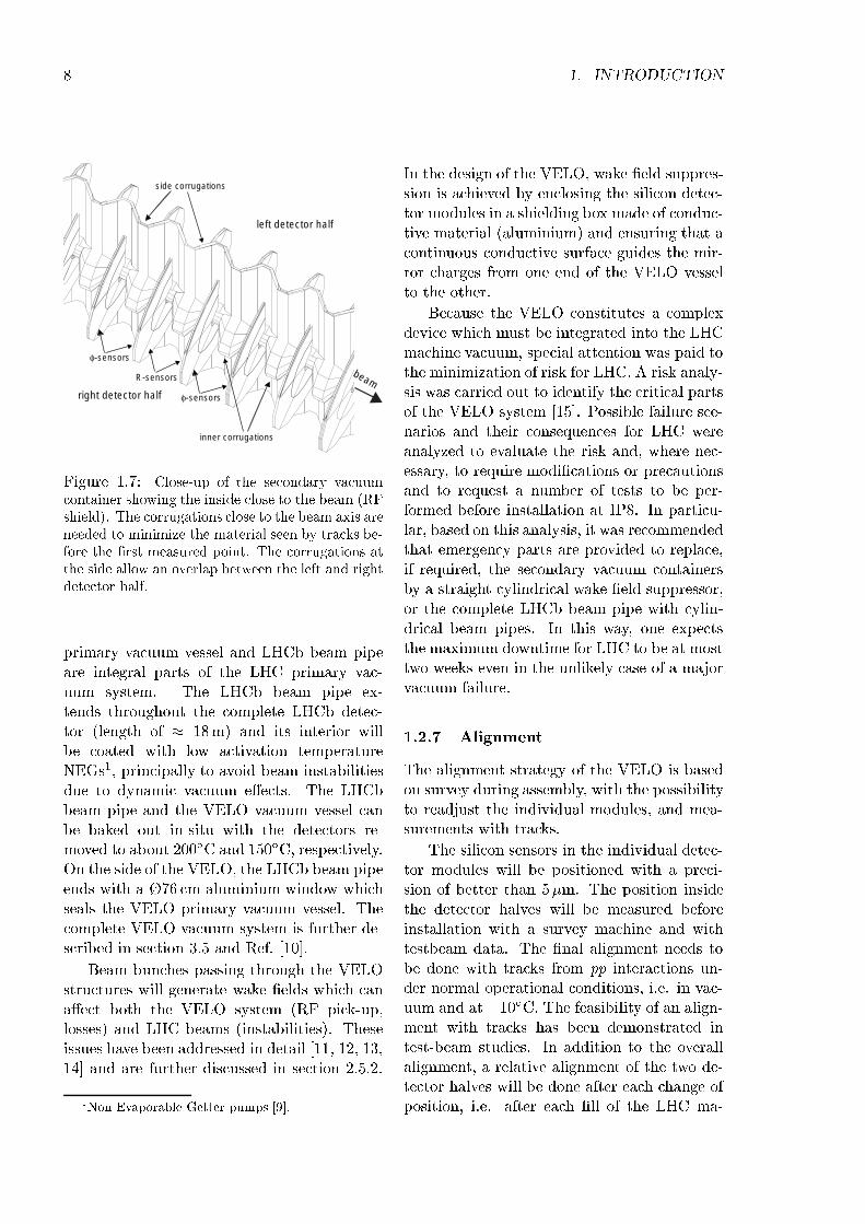
Figure 1.7: Close-up of the secondary vacuumcontainer showing the inside close to the beam (RFshield). The corrugations close to the beam axis areneeded to minimize the material seen by tracks be-fore the rst measured point. The corrugations atthe side allow an overlap between the left and rightdetector half.
primary vacuum vessel and LHCb beam pipeare integral parts of the LHC primary vac-uum system. The LHCb beam pipe ex-tends throughout the complete LHCb detec-tor (length of 18m) and its interior willbe coated with low activation temperatureNEGs1, principally to avoid beam instabilitiesdue to dynamic vacuum eects. The LHCbbeam pipe and the VELO vacuum vessel canbe baked out in-situ with the detectors re-moved to about 200ÆC and 150ÆC, respectively.On the side of the VELO, the LHCb beam pipeends with a 76 cm aluminium window whichseals the VELO primary vacuum vessel. Thecomplete VELO vacuum system is further de-scribed in section 3.5 and Ref. [10].
Beam bunches passing through the VELOstructures will generate wake elds which canaect both the VELO system (RF pick-up,losses) and LHC beams (instabilities). Theseissues have been addressed in detail [11, 12, 13,14] and are further discussed in section 2.5.2.
1Non Evaporable Getter pumps [9].
In the design of the VELO, wake eld suppres-sion is achieved by enclosing the silicon detec-tor modules in a shielding box made of conduc-tive material (aluminium) and ensuring that acontinuous conductive surface guides the mir-ror charges from one end of the VELO vesselto the other.
Because the VELO constitutes a complexdevice which must be integrated into the LHCmachine vacuum, special attention was paid tothe minimization of risk for LHC. A risk analy-sis was carried out to identify the critical partsof the VELO system [15]. Possible failure sce-narios and their consequences for LHC wereanalyzed to evaluate the risk and, where nec-essary, to require modications or precautionsand to request a number of tests to be per-formed before installation at IP8. In particu-lar, based on this analysis, it was recommendedthat emergency parts are provided to replace,if required, the secondary vacuum containersby a straight cylindrical wake eld suppressor,or the complete LHCb beam pipe with cylin-drical beam pipes. In this way, one expectsthe maximum downtime for LHC to be at mosttwo weeks even in the unlikely case of a majorvacuum failure.
1.2.7 Alignment
The alignment strategy of the VELO is basedon survey during assembly, with the possibilityto readjust the individual modules, and mea-surements with tracks.
The silicon sensors in the individual detec-tor modules will be positioned with a preci-sion of better than 5m. The position insidethe detector halves will be measured beforeinstallation with a survey machine and withtestbeam data. The nal alignment needs tobe done with tracks from pp interactions un-der normal operational conditions, i.e. in vac-uum and at 10ÆC. The feasibility of an align-ment with tracks has been demonstrated intest-beam studies. In addition to the overallalignment, a relative alignment of the two de-tector halves will be done after each change ofposition, i.e. after each ll of the LHC ma-
1.3. EVOLUTION SINCE THE TECHNICAL PROPOSAL 9
chine.
1.2.8 Material budget
The material which is placed within the LHCbacceptance, due to the dierent components ofthe VELO system is discussed in section 3.7.The main contributions come from the RFshield, silicon sensors and the exit window andamount on average to 9%, 5:3% and 1:9% of aradiation length respectively. A detailed studyof all the material can be found in Ref.[16].Special emphasis was put on minimizing thematerial before the rst measured point, whichresulted in a corrugated shape of the RF shield(Fig. 1.7).
1.2.9 Detector resolution
The errors on the track parameters arise fromthe intrinsic resolution of the detectors andfrom multiple Coulomb scattering, which inturn depends on the thickness of the materialin radiation lengths and the momentum of theparticle. The errors are magnied by the ex-trapolation distance from the rst measuredpoint to the vertex region and depend to rstorder on the transverse momentum of the par-ticle (section 4.4).
The error on the primary vertex is domi-nated by the number of tracks produced in app-collision. For an average event, the reso-lution in the z-direction is 42m and 10mperpendicular to the beam.
Impact parameter resolutions of 20m, ne-glecting the primary vertex contribution, areachieved for tracks with the highest transversemomentum.
The precision on the decay length rangesfrom 220m to 370m depending on the de-cay channel. A lifetime resolution of 40 fs isachieved for the B0
s ! Ds + decay channel,
which allows a 5 measurement of ms up to54 ps1 after one year of data-taking.
1.3 Evolution since the Technical
Proposal
Since the LHCb Technical Proposal [1] a majoreort went into the study of prototype detec-tors after heavy irradiation and the design ofa realistic vacuum system. Changes comparedto the TP are:
Sensors: In the TP, we proposed sixsensors of 60Æ coverage each per station.By reducing the outer radius of a sensorfrom 60mm to 42mm, it was possible toreduce the number to two sensors eachcovering 182Æ. As a consequence, thenumber of stations was increased from17 to 25. The inner radius was reducedfrom 10mm to 8mm.
The L1 electronics were moved behindthe shielding wall away from the high ra-diation environment.
Vacuum/Mechanics: A complete sys-tem design was carried out. This in-cludes a design of the vacuum vessel,motion and positioning mechanics, thin-walled structures for RF screening, sys-tems for cooling, vacuum, monitoringand control. Finite element analysis(FEA) was performed for the vessel andother components (exit window, coolingcapillaries, thin-walled detector encapsu-lation). Extensive prototyping was car-ried out on critical items, such as thethin-walled structures, vacuum protec-tion devices, large rectangular bellowsand the cooling system. The new designallows baking out of the primary vacuumsurfaces and provides easy access to thesilicon sensors.
Detector optimization: Detailedstudies were carried out of many dif-ferent detector designs to optimize thephysics performance. The layout wasnalized with 25 stations, with the ar-rangement as shown in Fig. 1.3, and withthe shape of the corrugations in the RF
10 1. INTRODUCTION
shield (Fig. 1.7) optimized for minimiz-ing multiple scattering.
1.4 Structure of this document
This Technical Design Report is intended to bea concise but self-contained description of theVELO system. Further details can be foundin the technical notes, which are referencedthroughout.
In Chapter 2 an overview is given of the re-sults obtained in the laboratory and test-beamusing prototypes, which give condence thatthe expected performance will be achieved.The technical design of the detectors is pre-sented in Chapter 3. The performance of theVELO system as obtained from simulation isdiscussed in Chapter 4. The issues of projectorganization, including the schedule and cost,are discussed in Chapter 5.
2 Summary of R&D and test of prototypes
2.1 Silicon
The complexities of the LHCb VELO sensordesign arise from the varying strip lengths, thedouble metal layer, and the need for regionsof very ne pitch. The rst aim of the pro-totyping programme was to ensure that thesensor gives the expected performance in thecontext of the chosen design. The second aimwas to check that this is maintained after ir-radiation. It should be noted that the moststringent requirements on the sensor perfor-mance are at low radius, where there is boththe nest pitch and the highest irradiation (seesection 4.3). The strong non-uniform natureof the irradiation is another special considera-tion for the LHCb VELO. The test-beam pro-gramme has also given the opportunity to testthe performance of the r-geometry in termsof the alignment and triggering requirementsfor LHCb.
The global performance of a sensor can becharacterized with the following inter-relatedparameters:
Signal to Noise Ratio: In order toensure eective trigger performance evenafter irradiation, the LHCb VELO aimsfor an initial signal to noise ratio, S/N,of more than 14 [17].
EÆciency: The goal for the eÆciencyis that it should be above 99% for S/N> 5.
Resolution: Typical resolutions whichcan be achieved are about 3:6m for100mrad tracks and 40m strip pitch.The resolution should not be degraded
by the irradiation nor by any aspect ofthe sensor design.
There are various constraints coming di-rectly from the strip layout which can aectthese parameters. The noise is aected by thelength of the strips and routing lines. The sizeof the signal can be aected by the presenceand geometry of the double metal layer, orthe capacitive coupling between strips. Otherconstraints come from the detailed technicaldesign, e.g. the strip capacitance will be af-fected by the thickness of dielectric separat-ing the two metal layers, the noise is aectedby the strip resistance, and so on. After ir-radiation the signal might be limited by thebreakdown voltage, or the onset of noise at aparticular bias voltage. The prototyping pro-gramme should establish that the design per-forms in the expected manner, both before andafter irradiation.
In addition there are various silicon tech-nology choices which can be made for a givenstrip layout.
2.1.1 Design parameters
The most important issues aecting the choiceof silicon technologies were investigated withdedicated LHCb prototyping, as described inthe following sections. The results were com-bined with knowledge available from the siliconliterature, in order to make the best choices forthe LHCb VELO. The principal considerationsare listed here.
Thickness
The voltage required to deplete the sensor isproportional to the square of the thickness.
11
12 2. SUMMARY OF R&D AND TEST OF PROTOTYPES
p implants+
n bulk
a) p side signal
electron drift
hole drift
traversing MIP
b)
Active region
p side signal
electron drift
hole drift
Undepleted insulating region
traversing MIP
c)p side signal
hole drift
electron drift
routing lineson 2nd metal layer
traversing MIP
d)
Active region
p side signal
electron drift
hole drift
Undepleted insulating region
traversing MIP
n implants+
n implants+
n implants+
p implants+
n implants+
dielectric
routing lineson 2nd metal layer
dielectric
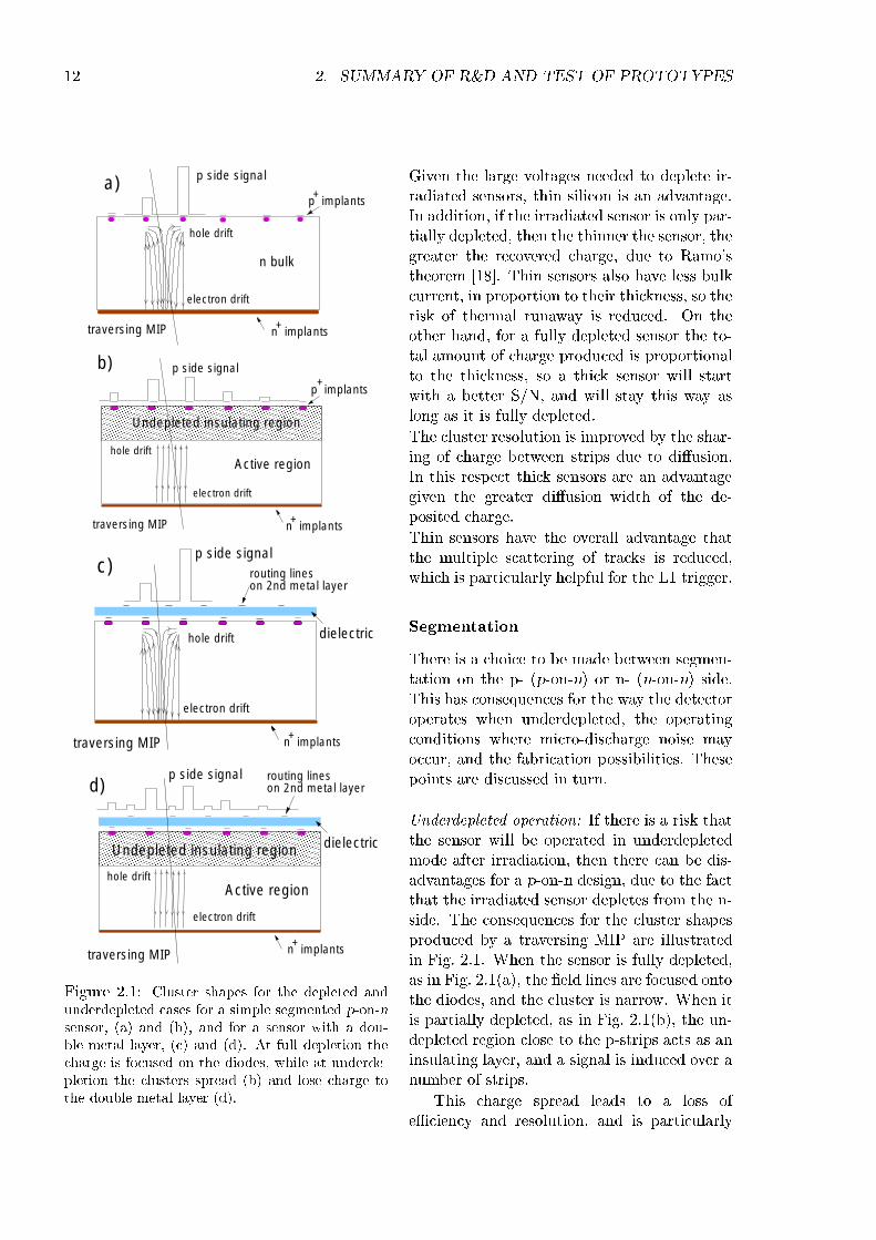
Figure 2.1: Cluster shapes for the depleted andunderdepleted cases for a simple segmented p-on-nsensor, (a) and (b), and for a sensor with a dou-ble metal layer, (c) and (d). At full depletion thecharge is focused on the diodes, while at underde-pletion the clusters spread (b) and lose charge tothe double metal layer (d).
Given the large voltages needed to deplete ir-radiated sensors, thin silicon is an advantage.In addition, if the irradiated sensor is only par-tially depleted, then the thinner the sensor, thegreater the recovered charge, due to Ramo'stheorem [18]. Thin sensors also have less bulkcurrent, in proportion to their thickness, so therisk of thermal runaway is reduced. On theother hand, for a fully depleted sensor the to-tal amount of charge produced is proportionalto the thickness, so a thick sensor will startwith a better S/N, and will stay this way aslong as it is fully depleted.
The cluster resolution is improved by the shar-ing of charge between strips due to diusion.In this respect thick sensors are an advantagegiven the greater diusion width of the de-posited charge.
Thin sensors have the overall advantage thatthe multiple scattering of tracks is reduced,which is particularly helpful for the L1 trigger.
Segmentation
There is a choice to be made between segmen-tation on the p- (p-on-n) or n- (n-on-n) side.This has consequences for the way the detectoroperates when underdepleted, the operatingconditions where micro-discharge noise mayoccur, and the fabrication possibilities. Thesepoints are discussed in turn.
Underdepleted operation: If there is a risk thatthe sensor will be operated in underdepletedmode after irradiation, then there can be dis-advantages for a p-on-n design, due to the factthat the irradiated sensor depletes from the n-side. The consequences for the cluster shapesproduced by a traversing MIP are illustratedin Fig. 2.1. When the sensor is fully depleted,as in Fig. 2.1(a), the eld lines are focused ontothe diodes, and the cluster is narrow. When itis partially depleted, as in Fig. 2.1(b), the un-depleted region close to the p-strips acts as aninsulating layer, and a signal is induced over anumber of strips.
This charge spread leads to a loss ofeÆciency and resolution, and is particularly
2.1. SILICON 13
dangerous for ne pitch sensors [19, 20]. Adouble metal layer can cause an additionalcharge loss, as illustrated in Fig. 2.1(c) and(d). These eects are not present for then-on-n design, where the depleted layer is onthe same side as the strips.
Micro-discharge noise: Micro-dischargenoise [21] is a reversible phenomenon ofrandom pulse noises around the edge of stripsfor bias voltages exceeding a certain value. Itis visible in the noise and the leakage current,and can place a limit on the bias voltagewhich can be applied to the sensor. Afterirradiation the high eld regions which causemicro-discharge noise are found close to then-strips [22] and so for an n-on-n design micro-discharge noise will occur at a lower voltagethan for the corresponding p-on-n design.The situation can however be improved witheld plates and rounded strips [23]. Beforeirradiation the situation is reversed, and theturn-on for micro-discharge in the p-on-ndesign will be at a lower voltage. In the LHCbVELO case, there is non-uniform irradiationacross the sensor, but only one voltage will beapplied. This bias voltage must be tuned tooptimize the charge collection eÆciency andnoise performance in all regions, which mayresult in areas of underdepletion. From thispoint of view, n-on-n is considered a saferdesign, as it gives a more reliable performancein situations of underdepletion, due to thereasons discussed in the previous paragraph.
Fabrication: p-on-n sensors have the advan-tage that the single-sided processing is easier,and it is possible to have a ner pitch due tothe fact that there is not the need to separatethe strips via a mechanism such as p-stops.However, it is possible to have a ne pitch forn-on-n sensors with the use of such techniquesas p-spray [24].
The segmentation choice is considered criticalfor LHCb, where the design includes ne pitchand double metal, and it has been investigatedextensively in the prototyping.
Oxygenation
Recent results from ROSE [25, 26] indicatethat there is an advantage to be gained by us-ing oxygenated silicon wafers. It was foundthat after irradiation the oxygenated sam-ples could be fully depleted with bias voltageswhich were both lower and more predictablethan for the standard samples. The advantagesare associated particularly with irradiation bycharged particles, which corresponds to the sit-uation in the LHCb VELO (see section 4.3).
Cryogenic operation
From considerations of annealing and leakagecurrent after irradiation, the sensors are ex-pected to operate at a temperature of 5ÆC(see section 3.1.1). The option of going to cryo-genic (liquid nitrogen) temperatures was alsoinvestigated. A possible advantage of cryo-genic operation is that due to trap lling thedepletion voltage of an irradiated sensor is low-ered. If the sensor is operating at underdeple-tion, the cryogenic temperatures can make itmore eÆcient and improve the resolution [19].However this is not a preferred solution forLHCb due to the fact that the recovery is lostafter a time interval of the order of minutes,and a very complex procedure would have tobe imagined to maintain the performance forlong time periods [19, 27].
Cryogenic operation also has an advantagein terms of lower leakage current, but at theVELO operating temperature the current isnot expected to be a dominant source of noise.After 3 years of operation the most irradiatedstrip, operated at 5ÆC, is expected to havea noise contribution from the current of 100electrons [28], which is less than 10% of thebaseline noise.
2.1.2 Prototype designs
This section summarizes the prototype designswhich have been tested for the LHCb VELO.There were three dierent types of geometricallayouts tested.
14 2. SUMMARY OF R&D AND TEST OF PROTOTYPES
p side n side
6 cm
3.4
cm
pitch = 42 µm
read
out p
itch
= 5
0 µm
strip
pitc
h =
25
µm
strips routing lines floating strips
DELPHI-ds sensor
Figure 2.2: Schematic of the DELPHI-ds proto-type.
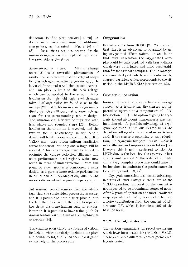
The DELPHI-ds prototype, manufac-tured by Hamamatsu1 is illustrated in Fig. 2.2.It is a double sided sensor with straight, or-thogonal strips. The main purpose of this pro-totype was to use an existing design to test theperformance of p-on-n and n-on-n ne pitchlayouts after non-uniform irradiation, in situa-tions of full depletion and under-depletion, andat cryogenic temperatures.
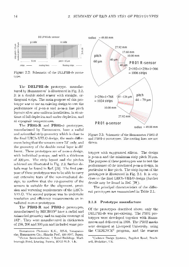
The PR01-R and PR01- prototypes,manufactured by Hamamatsu, have a radialand azimuthal strip geometry which is close tothe nal LHCb-VELO design, the main dier-ences being that the sensors cover 72Æ only, andthe geometry of the double metal layer is dif-ferent. These prototypes are of n-on-n design,with individual p-stops, and with a thicknessof 300m. The strip layout and the pitchesachieved are illustrated in Fig. 2.3; further de-tails may be found in Ref. [29]. The rst pur-pose of these prototypes was to be able to carryout extensive tests of the non-irradiated de-sign, to conrm that the r-geometry of thesensors is suitable for the alignment, preci-sion and vertexing requirements of the LHCb-VELO. The second purpose was to undertakeresolution and eÆciency measurements on ir-radiated n-on-n prototypes.
The PR02-R and PR02- prototypes,manufactured by MICRON2 have a radial andazimuthal geometry and an angular coverage of182Æ. They were manufactured in thicknessesof 150, 200 and 300 m and included some pro-
1Hamamatsu Photonics K.K., 325-6, Sunayama-cho, Hamamatsu City, Shizoka Pref., 430-8587, Japan.
2Micron Semiconductors, 1 Royal Buildings, Marl-borough Road, Lancing, Sussex, BN15 8UN, UK.
PR01 R-sensor
PR01 φ-sensor
2∗192+1∗256+1∗366= 1006 strips
1∗256+1∗768= 1024 strips 44 − 79 µm
60 µm40 µm
40 µm
45 −126 µm
= 49.88 mm
27.92 mm
10.00 mm
10.00 mm17.68 mm
27.92 mm
= 49.88 mm
pitch
radius
radius
pitch
Figure 2.3: Schematic of the Hamamatsu PR01-Rand PR01- prototypes. The routing lines are notshown.
totypes with oxygenated silicon. The designis p-on-n and the minimum strip pitch 24m.The purpose of these prototypes was to test theperformance of the irradiated p-on-n design, inparticular at ne pitch. The strip layout of theprototypes is illustrated in Fig. 2.4. It is veryclose to the nal LHCb-VELO design (furtherdetails may be found in Ref. [29]).
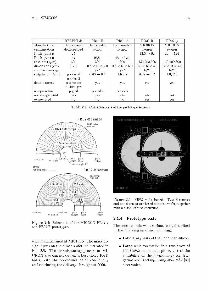
The principal characteristics of the dier-ent prototypes are summarized in Table 2.1.
2.1.3 Prototype manufacture
Of the prototypes described above, only theDELPHI-ds was pre-existing. The PR01 pro-totypes were developed together with Hama-matsu and delivered in 1998. The PR02 maskswere designed at Liverpool University, usingthe CADENCE3 program, and the sensors
3Cadence Design Systems, Bagshot Road, Brack-nell, Berkshire, UK.
2.1. SILICON 15
DELPHI-ds PR01-R PR01- PR02-R PR02-Manufacturer Hamamatsu Hamamatsu Hamamatsu MICRON MICRONsegmentation double-sided n-on-n n-on-n p-on-n p-on-nPitch (m) p 25 42:5! 92 24! 124Pitch (m) n 42 40,60 45! 126thickness (m) 300 300 300 150,200,300 150,200,300dimensions (cm) 3 6 0:8 < R < 5:0 0:8 < R < 5:0 0:8 < R < 4:0 0:8 < R < 4:0angular coverage 72Æ 72Æ 182Æ 182Æ
strip length (cm) p side: 6 0:63! 6:3 1.8,2.2 0:62! 6:3 1.0, 2.2n side: 3
double metal p side: no yes yes yes yesn side: yes
n-separation p-grid p-atolls p-atolls non-oxygenated yes yes yes yes yesoxygenated no no no yes yes
Table 2.1: Characteristics of the prototype sensors.
pitch24 µm
pitch55 µm
pitch124 µm
2048 stripsread out
PR02-φ sensor
r = 0.8 cmr = 2.22 cm
r = 4.0 cm pitch32.5 µm
pitch50 µm
pitch92 µm
PR02-R sensor
stereo angle 9 o
1024 outer strips
1024 inner strips
stripsrouting lines
256 strips
384strips
384strips
384strips
384strips
256 strips
r = 1.8 cmr = 0.8 cmr = 4.0 cm
2048 stripsread out
Figure 2.4: Schematic of the MICRON PR02-and PR02-R prototypes.
were manufactured at MICRON. The mask de-sign layout on the 6-inch wafer is illustrated inFig. 2.5. The manufacturing process at MI-CRON was carried out on a best eort R&Dbasis, with the procedures being continuallyrevised during the delivery throughout 2000.
Figure 2.5: PR02 wafer layout. Two R-sensorsand one sensor are tted onto the wafer, togetherwith a series of test structures.
2.1.4 Prototype tests
The sensors underwent various tests, describedin the following sections, including:
Laboratory tests of the unbonded silicon.
Large scale evaluation in a test-beam of120 GeV=c muons and pions, to test thesuitability of the r-geometry for trig-gering and tracking, using slow VA2 [30]electronics.
16 2. SUMMARY OF R&D AND TEST OF PROTOTYPES
Name Type Thickness Oxygenation Maximum Tests
m 1017 atoms=cm3 Irradiation1014 p=cm2
D-ds112 DELPHI-ds 310 None 3:5 TMX6, LAB
h1-R, h2-R,h4-R, h6-R, h7-R
PR01-R 300 None None TVA, LAB
h3-, h5-, h8-h9-, h11-, h12-
PR01- 300 None None TVA, LAB
h10-R PR01-R 300 None None TSCT, LAB
h-13-R PR01-R 300 None 3:4 TSCT
h-14- PR01- 300 None 4:1 TSCT
1976-21-b PR02-R 300 None None LAB
1968-17-c PR02-R 300 2.5 4:8 LSCT, LAB
1832-9-a PR02- 200 None 10:4 TSCT, LAB
Table 2.2: DELPHI-ds, PR01 and PR02 prototypes whose tests are described in this section. The testsare coded as follows: TVA: Test-beam evaluation with VA2 electronics, TMX6: Test-beam evaluationwith MX6 electronics, TSCT: Test-beam evaluation with SCT128A electronics, LSCT: Laser evaluationwith SCT128A electronics, LAB: Laboratory test.
Test-beam evaluation of non-irradiatedsilicon bonded to fast SCT128A [31] elec-tronics clocked at 40 MHz.
Non-uniform irradiation in a 24 GeV pro-ton beam followed by bonding to slow(MX6 [32] or VA2) or fast (SCT128A)electronics and evaluation both in thelaboratory and in a test-beam.
The list of prototype sensors for which de-tailed tests are discussed in this section is givenin Table 2.2.
2.1.5 Laboratory tests
PR01 Prototype
12 PR01 prototypes (h-1 to h-12) underwentlaboratory tests [33] at CERN. The depletionvoltage was measured from the C-V curve, theresistance of the set of strips to the back planewas checked, and the current versus voltagewas measured up to 200V. All sensors satis-ed the parameters given in Table 2.3. Afterbonding to VA2 hybrids the mean number ofdead channels was 0.8%.
PR02 Prototype
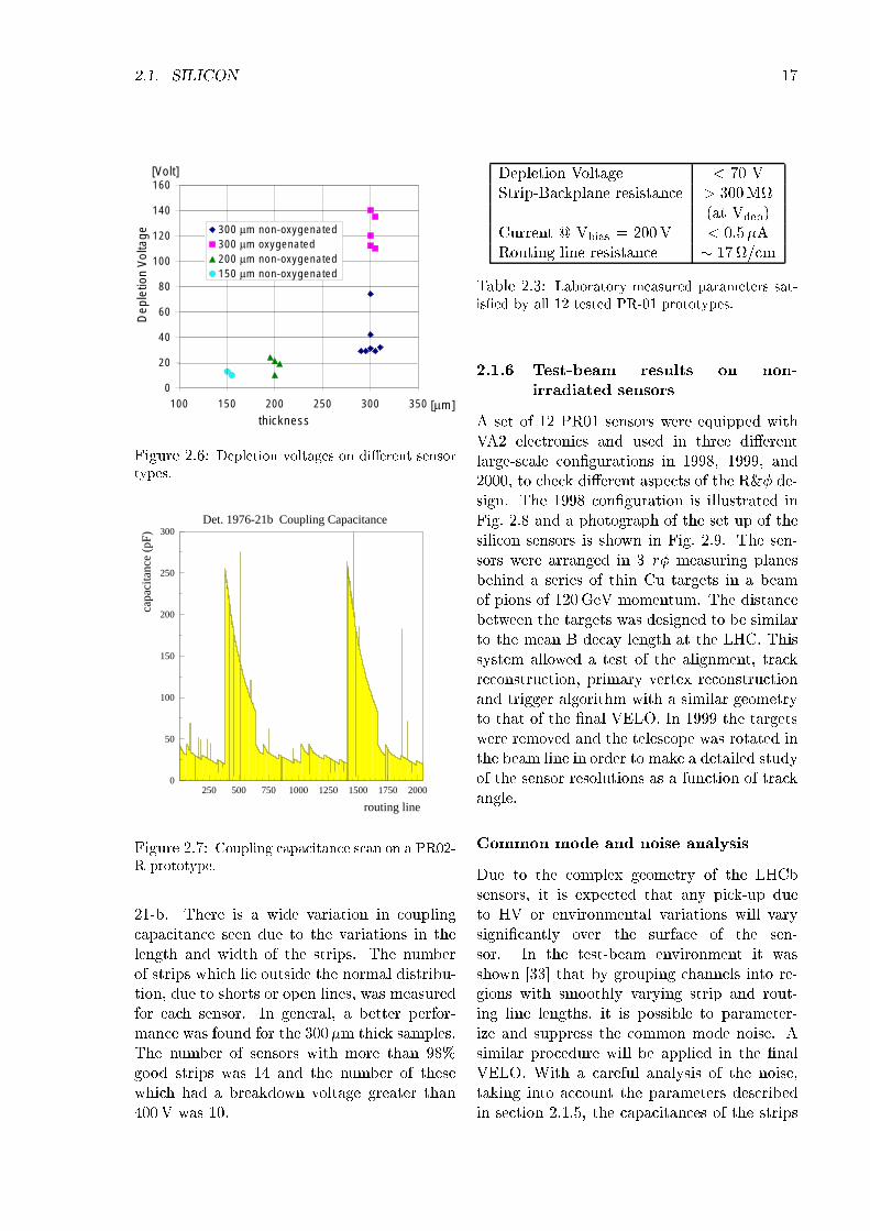
A total of 35 PR02 prototype sensors were de-livered from MICRON. The sensors covered arange of thicknesses, with 2, 10 and 23 detec-tors with thicknesses of 150, 200 and 300 mrespectively, and had dierent oxygenation lev-els, with 11 and 3 detectors oxygenated tolevels of 2:5 and 1:0 1017atoms=cm3 respec-tively. The pre-irradiation depletion voltageswere measured using a C-V scan. The val-ues measured for some dierent sensor typesare illustrated in Fig. 2.6. The pre-irradiationdepletion voltages are higher for the oxy-genated samples than for the non-oxygenatedones. The resistance of the routing lines wasmeasured on two sensors and found to be 23=cm.
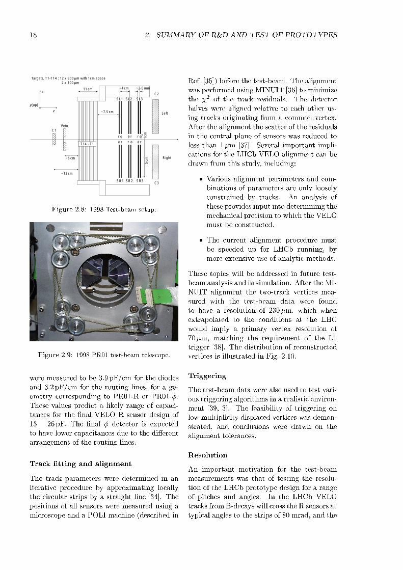
The breakdown voltages were determinedby slowly increasing the voltage until the cur-rent reached a maximum allowed value of15A. A total of 16 sensors were found tohave breakdown voltages above 400V, includ-ing both the oxygenated and non-oxygenatedsamples, and both of the thinnest (150m)sensors. The fraction of bad strips was mea-sured by probing the coupling capacitance ofeach strip. A typical output of such a scan isshown in Fig. 2.7 for the PR02-R sensor 1976-
2.1. SILICON 17
0
20
40
60
80
100
120
140
160
100 150 200 250 300 350
[Volt]
thickness[µm]
Dep
letio
n V
olta
ge 300 µm non-oxygenated300 µm oxygenated200 µm non-oxygenated150 µm non-oxygenated
Figure 2.6: Depletion voltages on dierent sensortypes.
Det. 1976-21b Coupling Capacitance
routing line
capa
cita
nce
(pF)
0
50
100
150
200
250
300
250 500 750 1000 1250 1500 1750 2000
Figure 2.7: Coupling capacitance scan on a PR02-R prototype.
21-b. There is a wide variation in couplingcapacitance seen due to the variations in thelength and width of the strips. The numberof strips which lie outside the normal distribu-tion, due to shorts or open lines, was measuredfor each sensor. In general, a better perfor-mance was found for the 300m thick samples.The number of sensors with more than 98%good strips was 14 and the number of thesewhich had a breakdown voltage greater than400V was 10.
Depletion Voltage < 70 VStrip-Backplane resistance > 300M
(at Vdep)Current @ Vbias = 200V < 0:5ARouting line resistance 17=cm
Table 2.3: Laboratory measured parameters sat-ised by all 12 tested PR-01 prototypes.
2.1.6 Test-beam results on non-irradiated sensors
A set of 12 PR01 sensors were equipped withVA2 electronics and used in three dierentlarge-scale congurations in 1998, 1999, and2000, to check dierent aspects of the R& de-sign. The 1998 conguration is illustrated inFig. 2.8 and a photograph of the set up of thesilicon sensors is shown in Fig. 2.9. The sen-sors were arranged in 3 r measuring planesbehind a series of thin Cu targets in a beamof pions of 120GeV momentum. The distancebetween the targets was designed to be similarto the mean B decay length at the LHC. Thissystem allowed a test of the alignment, trackreconstruction, primary vertex reconstructionand trigger algorithm with a similar geometryto that of the nal VELO. In 1999 the targetswere removed and the telescope was rotated inthe beam line in order to make a detailed studyof the sensor resolutions as a function of trackangle.
Common mode and noise analysis
Due to the complex geometry of the LHCbsensors, it is expected that any pick-up dueto HV or environmental variations will varysignicantly over the surface of the sen-sor. In the test-beam environment it wasshown [33] that by grouping channels into re-gions with smoothly varying strip and rout-ing line lengths, it is possible to parameter-ize and suppress the common mode noise. Asimilar procedure will be applied in the nalVELO. With a careful analysis of the noise,taking into account the parameters describedin section 2.1.5, the capacitances of the strips
18 2. SUMMARY OF R&D AND TEST OF PROTOTYPES
x
z
y(up)
~7.5 cm
~4 cm ~2-5 mm
1cm
5 cm
11 cm
Targets, T1-T14 : 12 x 300 µm with 1cm space 2 x 100 µm
C1Veto
C2
C3
r φr φ
r φrφrφ rφ
Left
Right
T14 - T1
SL1 SL2 SL3
SR1 SR2 SR3
~6 cm
~12 cm
Figure 2.8: 1998 Test-beam setup.
Figure 2.9: 1998 PR01 test-beam telescope.
were measured to be 3:9 pF/cm for the diodesand 3:2 pF/cm for the routing lines, for a ge-ometry corresponding to PR01-R or PR01-.These values predict a likely range of capaci-tances for the nal VELO R sensor design of13 26 pF. The nal detector is expectedto have lower capacitances due to the dierentarrangement of the routing lines.
Track tting and alignment
The track parameters were determined in aniterative procedure by approximating locallythe circular strips by a straight line [34]. Thepositions of all sensors were measured using amicroscope and a POLI machine (described in
Ref. [35]) before the test-beam. The alignmentwas performed using MINUIT [36] to minimizethe 2 of the track residuals. The detectorhalves were aligned relative to each other us-ing tracks originating from a common vertex.After the alignment the scatter of the residualsin the central plane of sensors was reduced toless than 1m [37]. Several important impli-cations for the LHCb VELO alignment can bedrawn from this study, including:
Various alignment parameters and com-binations of parameters are only looselyconstrained by tracks. An analysis ofthese provides input into determining themechanical precision to which the VELOmust be constructed.
The current alignment procedure mustbe speeded up for LHCb running, bymore extensive use of analytic methods.
These topics will be addressed in future test-beam analysis and in simulation. After the MI-NUIT alignment the two-track vertices mea-sured with the test-beam data were foundto have a resolution of 230m, which whenextrapolated to the conditions at the LHCwould imply a primary vertex resolution of70m, matching the requirement of the L1trigger [38]. The distribution of reconstructedvertices is illustrated in Fig. 2.10.
Triggering
The test-beam data were also used to test vari-ous triggering algorithms in a realistic environ-ment [39, 3]. The feasibility of triggering onlow multiplicity displaced vertices was demon-strated, and conclusions were drawn on thealignment tolerances.
Resolution
An important motivation for the test-beammeasurements was that of testing the resolu-tion of the LHCb prototype design for a rangeof pitches and angles. In the LHCb VELOtracks from B-decays will cross the R sensors attypical angles to the strips of 80 mrad, and the
2.1. SILICON 19
Entries 2310
z [cm]
0
20
40
60
80
-14 -12 -10 -8 -6 -4 -2 0
Figure 2.10: Reconstruction of primary verticesin the 1998 test-beam setup.
pitch track angle resolution
40m 80 120mrad 3:6 3:9m60m > 200mrad 4:0 4:6m
Table 2.4: Sensor resolution for two dierentpitches for the track angles giving best precision.
resolution is expected to benet from chargesharing. As the track angles are roughly par-allel to the strips this is not the case for the sensors.
In 1999 a dedicated test-beam run was per-formed with the telescope placed at varyingangles in the beam. The sensor resolution wasstudied as a function of incident angle [40].The best resolutions achieved in the PR01-Rsensor, which had two dierent pitches, aregiven in Table 2.4. It was shown that thecharge sharing for angled tracks leads to astrong variations in the resolution, as illus-trated in Fig. 2.11.
The PR01- sensors, which have pitchesvarying continuously from 45m to 126m,were used to study the resolution as a func-tion of pitch for perpendicular tracks [41]. Alinear dependence was found, with agreementwith the PR01-R sensors at 60m pitch. Forthe largest pitches the resolution is close to bi-
reso
lutio
n (µ
m)
0
1
2
3
4
5
6
7
8
9
10
telescope resolution, 40 µm pitch
test-beamsimulation
projected angle (rad)0 0.04 0.08 0.12 0.16 0.2 0.24
reso
lutio
n (µ
m)
0
2
4
6
8
10
12
14telescope resolution, 60 µm pitch
test-beamsimulation
Figure 2.11: Resolution as a function of track an-gle, as measured from the test-beam data for PR01-R sensors, and compared with the full simulation
nary, i.e. pitch=p12, whereas for the 45m
region there is signicant charge sharing andthe resolution is improved by a factor 2.
The results from the test-beam provide im-portant input to the simulation of the chargecollection process in the LHCb VELO silicondetectors. The modied simulation which willbe used takes into account the charge distribu-tion with full Landau modelling, lateral dif-fusion of charge carriers, knock-on electrons(Æ rays) and charge sharing between strips dueto capacitive coupling. The simulation wastuned to the test-beam data using a single freeparameter, the fraction of two strip clusters forperpendicular tracks. The agreement betweenthe improved model and the test-beam data isillustrated in Figs. 2.11 and 2.12.
SCT128A performance
The PR01 and PR02 prototypes were also usedin the test-beam to evaluate the SCT128A per-
20 2. SUMMARY OF R&D AND TEST OF PROTOTYPESfr
actio
n of
1-s
trip
clu
ster
s
0
0.1
0.2
0.3
0.4
0.5
0.6
0.7
0.8
0.9
1
test-beam, 40 µm pitch
test-beam, 60 µm pitch
simulation
fraction of 2-strip clusters
projected angle (rad)0 0.04 0.08 0.12 0.16 0.2
frac
tion
of 3
-str
ip c
lust
ers
0
0.1
0.2
0.3
0.4
0.5
0.6
0.7
0.8
0.9
projected angle (rad)0 0.04 0.08 0.12 0.16 0.2 0.24
fraction of >=4-strip clusters
Figure 2.12: Simulated fractions of 1, 2, 3, andn-strip (n 4) clusters versus track angle for twodierent strip pitches, for data and simulation.
63.70 mm
38.2
0 m
m
Figure 2.13: Layout of the 6-chip hybrid.
formance. For this purpose, and for testing theirradiated detectors, specially designed fan-insand hybrids were fabricated. The fan-ins weremanufactured on glass (1999 test-beam) andon ceramic (2000 test-beam). Two hybrid de-signs were used, which could accommodate 3or 6 chips. The layout of the 6-chip hybrid isillustrated in Fig. 2.13.
The best S/N measured with the SCT128Aand a 300m thick detector was 21:5. The re-
sults of the evaluation of the SCT128A pulse-shape are discussed in section 2.4.1.
2.1.7 Irradiation procedures
For the LHCb VELO prototyping a non-uniform irradiation was used. As the radi-ation damage will be dominated by chargedparticles, an irradiation in the 24 GeV protonPS beam was appropriate. The sensors werestationary throughout the irradiation with ei-ther a perpendicular or horizontal orientationwith respect to the beam. The beam prolewas measured to be a gaussian of a width of6:10:3mm, hence a less irradiated region wasalways contained within the sensor. The dosewas monitored during the irradiation using sec-ondary emission counters, and was measuredafter the irradiation was nished by measuringthe activity of small pieces of pure Al placed infront of and behind the sensor. As an example,Fig. 2.21 shows a schematic of the irradiationof sensor 1832-9-a. After the irradiation thesensor was equipped with electronics allowingareas from both the irradiated and the non-irradiated sides to be read out. More detailsabout the irradiation can be found in Ref. [42].The sensors were fully benecially annealed af-ter the irradiation, with the consequence thatthey were tested in a condition where a doseof 2 1014 p=cm2 24 GeV protons correspondsto approximately one year of running for theinnermost part of the VELO sensors.
2.1.8 Test-beam results on irradiatedsensors
In the year 2000 the test-beam setup was mod-ied to be suitable for testing irradiated sen-sors equipped with fast electronics. A cold box ushed with nitrogen was placed behind thetelescope. Behind this box a second telescopewas installed, consisting of 3 sensors, placed atangles to optimize the resolution. The trig-ger was provided by the coincidence of twoscintillators. One of the telescope sensors wasequipped with fast SCT128A electronics, so inthe case of multiple track events the correct in-time track could be identied. A photograph of
2.1. SILICON 21
N2
x
z
Beam
1 m
Dark box
Rφ Rφ φ R
First telescope station
resolution: 5 µm
VA2 readoutCooling
oil
irradiated sensor
Second telescope station
resolution: 5 µm
Trig
ger
scin
tilla
tor
yRR φ
VA
2
SC
T12
8A
Cold box
Trig
ger
scin
tilla
tor
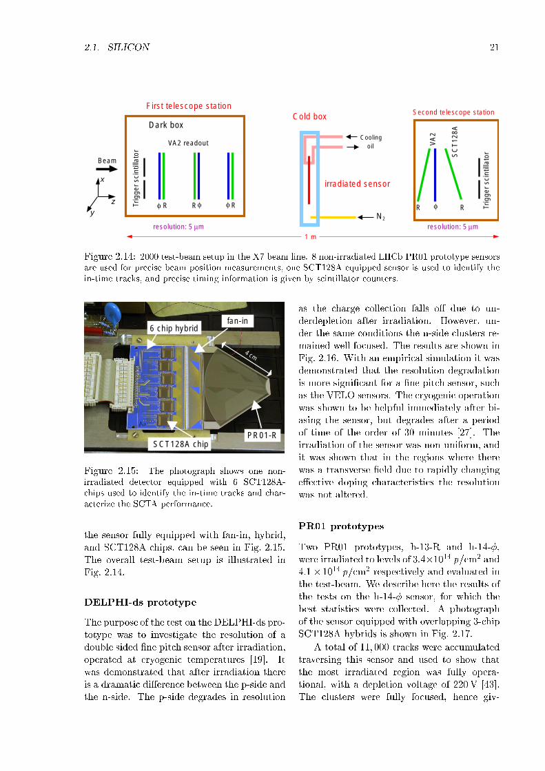
Figure 2.14: 2000 test-beam setup in the X7 beam line. 8 non-irradiated LHCb PR01 prototype sensorsare used for precise beam position measurements, one SCT128A equipped sensor is used to identify thein-time tracks, and precise timing information is given by scintillator counters.
SCT128A chip
6 chip hybridfan-in
PR01-R
4 cm
Figure 2.15: The photograph shows one non-irradiated detector equipped with 6 SCT128A-chips used to identify the in-time tracks and char-acterize the SCTA performance.
the sensor fully equipped with fan-in, hybrid,and SCT128A chips, can be seen in Fig. 2.15.The overall test-beam setup is illustrated inFig. 2.14.
DELPHI-ds prototype
The purpose of the test on the DELPHI-ds pro-totype was to investigate the resolution of adouble sided ne pitch sensor after irradiation,operated at cryogenic temperatures [19]. Itwas demonstrated that after irradiation thereis a dramatic dierence between the p-side andthe n-side. The p-side degrades in resolution
as the charge collection falls o due to un-derdepletion after irradiation. However, un-der the same conditions the n-side clusters re-mained well focused. The results are shown inFig. 2.16. With an empirical simulation it wasdemonstrated that the resolution degradationis more signicant for a ne pitch sensor, suchas the VELO sensors. The cryogenic operationwas shown to be helpful immediately after bi-asing the sensor, but degrades after a periodof time of the order of 30 minutes [27]. Theirradiation of the sensor was non-uniform, andit was shown that in the regions where therewas a transverse eld due to rapidly changingeective doping characteristics the resolutionwas not altered.
PR01 prototypes
Two PR01 prototypes, h-13-R and h-14-,were irradiated to levels of 3:41014 p=cm2 and4:1 1014 p=cm2 respectively and evaluated inthe test-beam. We describe here the results ofthe tests on the h-14- sensor, for which thebest statistics were collected. A photographof the sensor equipped with overlapping 3-chipSCT128A hybrids is shown in Fig. 2.17.
A total of 11; 000 tracks were accumulatedtraversing this sensor and used to show thatthe most irradiated region was fully opera-tional, with a depletion voltage of 220 V [43].The clusters were fully focused, hence giv-
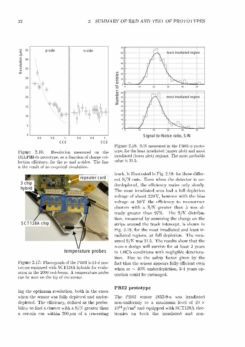
22 2. SUMMARY OF R&D AND TEST OF PROTOTYPES
p-side n-side
CCECCE
Res
olut
ion
(µm
) 45
0.8 1.0.60
5
10
15
20
25
30
35
40
0.8 1.0.6
Figure 2.16: Resolution measured on theDELPHI-ds prototype, as a function of charge col-lection eÆciency, for the p- and n-sides. The lineis the result of an empirical simulation.
SCT128A chip
repeater card3 chiphybrid
temperature probes
Figure 2.17: Photograph of the PR01 h-14- pro-totype equipped with SCT128A hybrids for evalu-ation in the 2000 test-beam. A temperature probecan be seen on the tip of the sensor.
ing the optimum resolution, both in the caseswhen the sensor was fully depleted and under-depleted. The eÆciency, dened as the proba-bility to nd a cluster with a S/N greater thana certain cut within 200 m of a traversing
0
10
20
30
40
50
60
70
least irradiated region
0 10 20 30 40 500
5
10
15
20
25
30
35
40
most irradiated region
Num
ber
of e
ntrie
s
Signal to-Noise ratio, S/N
0 10 20 30 40 50
Figure 2.18: S/N measured in the PR01- proto-type, for the least irradiated (upper plot) and mostirradiated (lower plot) regions. The most probablevalue is 21:5 .
track, is illustrated in Fig. 2.19, for three dier-ent S/N cuts. Even when the detector is un-derdepleted, the eÆciency varies only slowly.The most irradiated area had a full depletionvoltage of about 220 V, however with the biasvoltage at 50V the eÆciency to reconstructclusters with a S/N greater than 5 was al-ready greater than 97%. The S/N distribu-tion, measured by summing the charge on thestrips around the track intercept, is shown inFig. 2.18, for the most irradiated and least ir-radiated regions, at full depletion. The mea-sured S/N was 21:5. The results show that then-on-n design will survive for at least 2 yearsin LHCb conditions with negligible deteriora-tion. Due to the safety factor given by thefact that the sensor appears fully eÆcient evenwhen at 40% underdepletion, 3-4 years op-eration could be envisaged.
PR02 prototype
The PR02 sensor 1832-9-a was irradiatednon-uniformly to a maximum level of 10 1014 p=cm2 and equipped with SCT128A elec-tronics on both the irradiated and non-
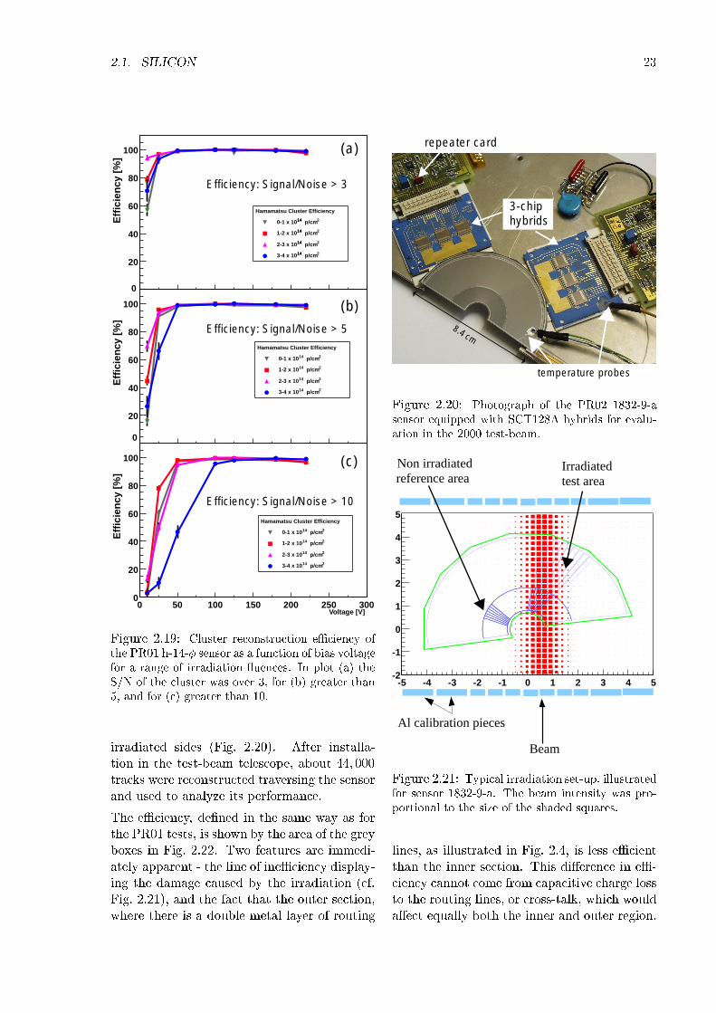
2.1. SILICON 23
Eff
icie
ncy
[%
]
0
20
40
60
80
100
Efficiency: Signal/Noise > 5
Voltage [V]0 50 100 150 200 250 300
Eff
icie
ncy
[%
]
0
20
40
60
80
100
Efficiency: Signal/Noise > 10
Eff
icie
ncy
[%
]
0
20
40
60
80
100
Efficiency: Signal/Noise > 3
Hamamatsu Cluster Efficiency
0-1 x 10
1-2 x 10
2-3 x 10
3-4 x 10
(a)
(b)
1414 2p/cm
1414 2p/cm
1414 2p/cm
1414 2p/cm
Hamamatsu Cluster Efficiency
0-1 x 10
1-2 x 10
2-3 x 10
3-4 x 10
14 2p/cm
14 2p/cm
14 2p/cm
14 2p/cm
Hamamatsu Cluster Efficiency
0-1 x 10
1-2 x 10
2-3 x 10
3-4 x 10
14 2p/cm
14 2p/cm
14 2p/cm
14 2p/cm
(c)
Figure 2.19: Cluster reconstruction eÆciency ofthe PR01 h-14- sensor as a function of bias voltagefor a range of irradiation uences. In plot (a) theS/N of the cluster was over 3, for (b) greater than5, and for (c) greater than 10.
irradiated sides (Fig. 2.20). After installa-tion in the test-beam telescope, about 44; 000tracks were reconstructed traversing the sensorand used to analyze its performance.
The eÆciency, dened in the same way as forthe PR01 tests, is shown by the area of the greyboxes in Fig. 2.22. Two features are immedi-ately apparent - the line of ineÆciency display-ing the damage caused by the irradiation (cf.Fig. 2.21), and the fact that the outer section,where there is a double metal layer of routing
repeater card
3-chiphybrids
8.4 cm
temperature probes
Figure 2.20: Photograph of the PR02 1832-9-asensor equipped with SCT128A hybrids for evalu-ation in the 2000 test-beam.
-5 -4 -3 -2 -1 0 1 2 3 4 5-2
-1
0
1
2
3
4
5
Non irradiatedreference area
Irradiated test area
Al calibration pieces
Beam
Figure 2.21: Typical irradiation set-up, illustratedfor sensor 1832-9-a. The beam intensity was pro-portional to the size of the shaded squares.
lines, as illustrated in Fig. 2.4, is less eÆcientthan the inner section. This dierence in eÆ-ciency cannot come from capacitive charge lossto the routing lines, or cross-talk, which wouldaect equally both the inner and outer region.
24 2. SUMMARY OF R&D AND TEST OF PROTOTYPES
x [cm]-5 -4 -3 -2 -1 0 1 2 3 4 5
y [c
m]
-2
-1
0
1
2
3
4
5
300VOuter region
Inner region
Figure 2.22: EÆciency of the PR02 1832-9-a sen-sor at Vbias=300V. The size of the boxes is pro-portional to the eÆciency. The irradiated side ofthe sensor shows an ineÆciency along the line ofthe irradiation. The additional eect of charge lossto the double metal layer, which is only present inthe outer region, is also clearly visible.
It is a signature of an underdepleted layer nextto the p-strips, as illustrated in Fig. 2.1. Dueto the unique geometry of this sensor it is pos-sible to measure the charge picked up in thedouble metal layer, as the lines concerned runparallel to the strips. The measurement is il-lustrated in Fig. 2.23. When the sensor is un-derdepleted the charge picked up in the secondmetal layer rises to 20%. Note that for the Rgeometry, where the double metal lines crossthe strips perpendicularly, any lost charge isunrecoverable. It was shown [44] that the clus-ters spread, as illustrated in Fig. 2.1, and theresolution will degrade as soon as the sensorbecomes underdepleted.
For the same reasons the sensor eÆciencyalso shows a very sharp dependence on biasvoltage and irradiation. In Fig. 2.24 the eÆ-ciency measured at a bias voltage of 300V isillustrated for dierent irradiation levels.
In the regions with a dose correspondingto about one year of LHCb operation, the de-pletion voltage rose to about 300V, which isrelatively high for a 200m thick sensor.
0
5
10
15
20
25 stripsrouting lines
0 2 4 6 8 10-0.2
-0.1
-0
0.1
0.2
0.3
0.4
Sign
al [
AD
C c
ount
s]fr
actio
n in
rou
ting
lines
Inner Region
stripsrouting lines
0 2 4 6 8 10 12
Outer Region
Irradiation [x 10 p /cm ]14 2
Irradiation [x 10 p /cm ]14 2
Figure 2.23: Charge from strips, routing lines, andthe relative fraction (dened as routing line chargedivided by total charge), for the inner (left) andouter (right) regions, at Vbias = 300V.
0 2 4 6 8 10 120
20
40
60
80
100S/N > 3
S/N > 5
S/N > 10
Efficiency in outer region at 300 V
Effi
cien
cy [%
]
Irradiation [x 10 p /cm ]14 2
Figure 2.24: EÆciency of the PR02- 1832-9-aouter region at Vbias = 300V vs. irradiation.
2.1.9 Measurements with a laser
In addition to the measurements with a highenergy beam, an infrared laser system wasused for detailed performance studies [45]. Anoxygenated p-on-n PR02-R sensor, 1968-17-c, non-uniformly irradiated up to a maximumlevel of 4:8 1014 p=cm2 of 24 GeV protons,was characterized. The sensor was read out
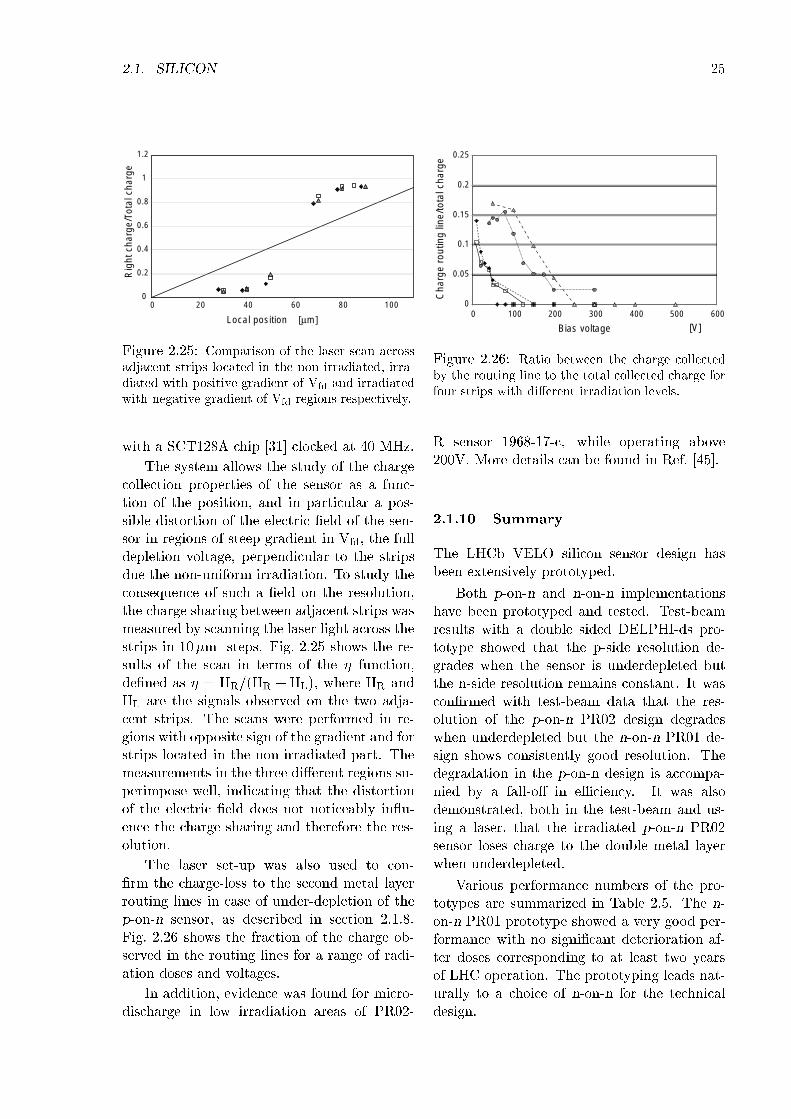
2.1. SILICON 25
0
0.2
0.4
0.6
0.8
1
1.2
0 20 40 60 80 100
Rig
ht c
harg
e/To
tal c
harg
e
Local position [µm]
Figure 2.25: Comparison of the laser scan acrossadjacent strips located in the non irradiated, irra-diated with positive gradient of Vfd and irradiatedwith negative gradient of Vfd regions respectively.
with a SCT128A chip [31] clocked at 40 MHz.
The system allows the study of the chargecollection properties of the sensor as a func-tion of the position, and in particular a pos-sible distortion of the electric eld of the sen-sor in regions of steep gradient in Vfd, the fulldepletion voltage, perpendicular to the stripsdue the non-uniform irradiation. To study theconsequence of such a eld on the resolution,the charge sharing between adjacent strips wasmeasured by scanning the laser light across thestrips in 10m steps. Fig. 2.25 shows the re-sults of the scan in terms of the function,dened as = HR=(HR +HL), where HR andHL are the signals observed on the two adja-cent strips. The scans were performed in re-gions with opposite sign of the gradient and forstrips located in the non-irradiated part. Themeasurements in the three dierent regions su-perimpose well, indicating that the distortionof the electric eld does not noticeably in u-ence the charge sharing and therefore the res-olution.
The laser set-up was also used to con-rm the charge-loss to the second metal layerrouting lines in case of under-depletion of thep-on-n sensor, as described in section 2.1.8.Fig. 2.26 shows the fraction of the charge ob-served in the routing lines for a range of radi-ation doses and voltages.
In addition, evidence was found for micro-discharge in low irradiation areas of PR02-
0
0.05
0.1
0.15
0.2
0.25
0 100 200 300 400 500 600
Cha
rge
rout
ing
line/
tota
l cha
rge
Bias voltage [V]
Figure 2.26: Ratio between the charge collectedby the routing line to the total collected charge forfour strips with dierent irradiation levels.
R sensor 1968-17-c, while operating above200V. More details can be found in Ref. [45].
2.1.10 Summary
The LHCb VELO silicon sensor design hasbeen extensively prototyped.
Both p-on-n and n-on-n implementationshave been prototyped and tested. Test-beamresults with a double sided DELPHI-ds pro-totype showed that the p-side resolution de-grades when the sensor is underdepleted butthe n-side resolution remains constant. It wasconrmed with test-beam data that the res-olution of the p-on-n PR02 design degradeswhen underdepleted but the n-on-n PR01 de-sign shows consistently good resolution. Thedegradation in the p-on-n design is accompa-nied by a fall-o in eÆciency. It was alsodemonstrated, both in the test-beam and us-ing a laser, that the irradiated p-on-n PR02sensor loses charge to the double metal layerwhen underdepleted.
Various performance numbers of the pro-totypes are summarized in Table 2.5. The n-on-n PR01 prototype showed a very good per-formance with no signicant deterioration af-ter doses corresponding to at least two yearsof LHC operation. The prototyping leads nat-urally to a choice of n-on-n for the technicaldesign.
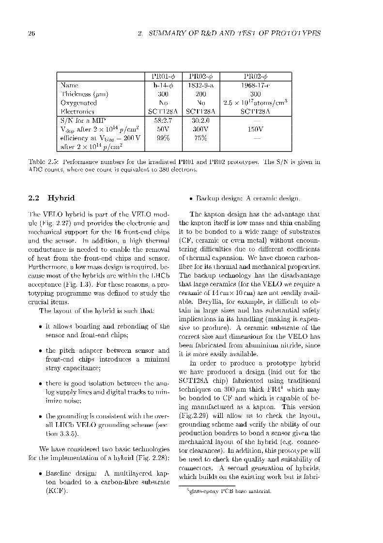
26 2. SUMMARY OF R&D AND TEST OF PROTOTYPES
PR01- PR02- PR02-
Name h-14- 1832-9-a 1968-17-cThickness (m) 300 200 300Oxygenated No No 2:5 1017atoms=cm3
Electronics SCT128A SCT128A SCT128A
S/N for a MIP 58:2.7 30:2.0 Vdep after 2 1014 p=cm2 50V 300V 150VeÆciency at Vbias = 200V 99% 75% after 2 1014 p=cm2
Table 2.5: Performance numbers for the irradiated PR01 and PR02 prototypes. The S/N is given inADC counts, where one count is equivalent to 380 electrons.
2.2 Hybrid
The VELO hybrid is part of the VELO mod-ule (Fig. 2.27) and provides the electronic andmechanical support for the 16 front-end chipsand the sensor. In addition, a high thermalconductance is needed to enable the removalof heat from the front-end chips and sensor.Furthermore, a low mass design is required, be-cause most of the hybrids are within the LHCbacceptance (Fig. 1.3). For these reasons, a pro-totyping programme was dened to study thecrucial items.
The layout of the hybrid is such that:
it allows bonding and rebonding of thesensor and front-end chips;
the pitch adapter between sensor andfront-end chips introduces a minimalstray capacitance;
there is good isolation between the ana-log supply lines and digital tracks to min-imize noise;
the grounding is consistent with the over-all LHCb VELO grounding scheme (sec-tion 3.3.5).
We have considered two basic technologiesfor the implementation of a hybrid (Fig. 2.28):
Baseline design: A multilayered kap-ton bonded to a carbon-bre substrate(KCF).
Backup design: A ceramic design.
The kapton design has the advantage thatthe kapton itself is low mass and thin enablingit to be bonded to a wide range of substrates(CF, ceramic or even metal) without encoun-tering diÆculties due to dierent coeÆcientsof thermal expansion. We have chosen carbon-bre for its thermal and mechanical properties.The backup technology has the disadvantagethat large ceramics (for the VELO we require aceramic of 14 cm 10 cm) are not readily avail-able. Beryllia, for example, is diÆcult to ob-tain in large sizes and has substantial safetyimplications in its handling (making it expen-sive to produce). A ceramic substrate of thecorrect size and dimensions for the VELO hasbeen fabricated from aluminium nitride, sinceit is more easily available.
In order to produce a prototype hybridwe have produced a design (laid out for theSCT128A chip) fabricated using traditionaltechniques on 300 m thick FR44 which maybe bonded to CF and which is capable of be-ing manufactured as a kapton. This version(Fig.2.29) will allow us to check the layout,grounding scheme and verify the ability of ourproduction bonders to bond a sensor given themechanical layout of the hybrid (e.g. connec-tor clearances). In addition, this prototype willbe used to check the quality and suitability ofconnectors. A second generation of hybrids,which builds on the existing work but is fabri-
4glass-epoxy PCB base material.
2.3. VELO MODULES 27
Sensor
Hybrid
Paddle
Front-end chips
thermal contact
adjustment screws
Figure 2.27: One VELOModule, showing the sen-sor and the hybrid with 16 front-end chips.
TPG
Chipkapton
sensor
CF weave
CF(UD)
Chipkapton
sensor
TPG
CF weave
CF(UD)
Chipkaptonsensor
ceramic
TPG
Chipkaptonsensor
ceramic
TPG
KCF design (baseline):
Ceramic design (backup):
Figure 2.28: Schematics of the two hybrid designs.
cated on kapton, is under design. This hybridwill be able to carry the SCTA VELO chip.
2.3 VELO modules
The thermal properties of the LHCb VELOmodule are vital to control the operating tem-perature of the VELO sensors. The VELO de-tectors will be exposed to a maximum ux ofparticles equivalent to 0:51:31014 neq/cm
2
per year, which will lead to increased deple-tion voltage and bulk current. The total powerdissipation per sensor is expected to stay be-low 0:3W when operating the detector below0ÆC during their lifetime. However all heat
footprints for 16 chips
area for sensor
area for pitch adapter
connector forbias voltage for sensor and chipstiming and control signals
connector foranalog signals
Figure 2.29: Photograph of a prototype PCB-hybrid for SCT128A chip.
will be dissipated close to the beam-line, andthe silicon itself will be used to provide thethermal link to the edge of the sensor to avoidextra material. Power dissipation in the sil-icon bulk heats the detector causing a localincrease in bulk current, which will then resultin larger currents. At temperatures below 0ÆCthe currents will not contribute signicantly tothe electronics noise, however increased powerdissipation due to higher currents could leadto thermal runaway. On the long term highertemperatures will lead to larger depletion volt-ages. The main power dissipation is due tothe readout electronics of the VELO detector,which is designed to stay below 12W per hy-brid. Hence the total power dissipation in amodule will be 24W. Applying a safety factorof 1:5, the cooling system should be able tocope with 36W per module.
The prototype module design [46] incorpo-rates several key features to be able to guar-antee the desired operating temperature of thesilicon sensor and electronics.
A carbon bre (CF) weave substratethat carries the front-end electron-ics and provides the mechanical andthermal link to the sensors. TheCF is bonded with a thin (300m)layer of thermo-pyrolytic graphite(TPG, 1700Wm1K1) and a layer
28 2. SUMMARY OF R&D AND TEST OF PROTOTYPES
Video probe
marble table
module prototype
cooling pipe
heating elements
adjustment screws
y
z
x
slew
roll
pitch
Figure 2.30: Photograph of a module prototypewhich is used for alignment studies and thermaltests. The video probe of the survey machine isalso seen.
of highly conductive (600Wm1K1)uni-directional carbon bre that carriesthe sensors.
A connection to the CO2 cooling systemis made through an aluminium (or tita-nium) coupler and a soft-metal indiumjoint.
The sensors are bonded to the CF usinga 100m thick glue layer. The lengthof the glue bond is a parameter of theprototyping, since it has to strike a bal-ance between good heat transfer and de-formation due to dierent expansion co-eÆcients.
A thermal simulation [47] of the modulehas been performed to establish that the pro-totype is capable of keeping the sensors in thetemperature range 10Æ to 0ÆC. The ANSYS 5
5ANSYS 5.6, ANSYS Inc., http://www.ansys.com
Infrared camera
Infrared transparent window
Vacuum chamber
Figure 2.31: Photograph of the vacuum chamberand the infrared camera used for the thermal mea-surements.
program was used to model the temperatureprole of the sensors under the expected andrequired thermal loads of 24W and 36W fromthe front-end chips. A conservative estimate of0:3W in the silicon and a CO2 cooling temper-ature of 25ÆC was assumed. Table 2.6 showsthe results of the simulation. In the CF hybridbaseline design using a full glue bond the sili-con is kept below the required operating tem-perature. The backup designs also fulll thisrequirement.
Measurements of the temperature prole ofthe silicon were made using an infrared (IR)camera and a prototype module constructedwith an aluminium nitride substrate. Themodule was operated in vacuum (Fig. 2.31)in order to remove convective cooling (sim-ulating the LHCb environment). The FE-electronics were replaced with small heatingelements. Figure 2.32 shows an IR photographfor a power dissipation of 4W in the heatingelements. Preliminary results show agreementbetween simulation and the measurements per-formed with the IR-camera to within 1ÆC.
Two prototype modules with aluminiumnitride substrates have been built. Using anon-contact method with a video probe at-tached to a coordinate measuring machine(Fig. 2.30) it has been shown that the sensorsmay be reproducibly positioned relative to thelocation surfaces to a precision of about 5m
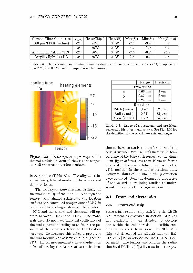
2.4. FRONT-END ELECTRONICS 29
Carbon Fibre Composite Tcool Heat(Chips) Heat(Si) Max(Si) Min(Si) Max(Chips)
300 m TPG(baseline) -25 24W 0.3W -7.3 -9.9 3.3
-25 36W 0.3W -4.2 -7.0 8.9
Aluminium Nitride/TPG -25 36W 0.3W -7.5 -8.2 24.5
Beryllia Hybrid/TPG -25 36W 0.3W -7.5 -9.6 2.7
Table 2.6: The maximum and minimum temperatures on the sensors and chips for a CO2 temperatureof 25ÆC, and 0:3W power dissipation in the sensors.
cooling tube heating elements
sensor
-5
-10
-15
-20
C0
Figure 2.32: Photograph of a prototype VELOthermal module (in vacuum) showing the temper-ature distribution on the front surface.
in x, y and z (Table 2.7). The alignment in-volved using ducial marks on the sensors anddepth of focus.
The prototypes were also used to check thethermal stability of the module. Although thesensors were aligned relative to the locationsurfaces at a controlled temperature of 23ÆC inoperation the cooling system will be at about20ÆC and the sensors and electronic will op-erate between 10ÆC and +10ÆC. The mate-rials used do not have identical coeÆcients ofthermal expansion leading to shifts in the po-sition of the sensors relative to the locationsurfaces. To measure this eect a prototypethermal module was assembled and aligned at21ÆC. Initial measurements have studied theeect of heating the base relative to the loca-
Range Precision
Translations
x 0:66mm 4my 0:87mm 6mz 0:24mm 3m
Rotations
Pitch (x-axis) 0:76Æ 52radRoll (y-axis) 0:52Æ 35radSlew (z-axis) 1:76Æ 35rad
Table 2.7: Range of adjustments and precisionsachieved with adjustment screws. See Fig. 2.30 forthe denition of the coordinate axis and angles.
tion surfaces to study the performance of thebase structure. With a 10ÆC increase in tem-perature of the base with respect to the align-ment jig (platform) less than 10m shift wasobserved in the sensor ducial relative to the21ÆC position in the x and zpositions only.However, shifts of 100m in the ydirectionwere observed. Both the design and propertiesof the materials are being studied to under-stand the source of this large movement.
2.4 Front-end electronics
2.4.1 Front-end chip
Since a fast readout chip satisfying the LHCbrequirement as discussed in section 3.3.2 wasnot available, it was decided to developone within the collaboration. Possible can-didates to start from were the SCT128Achip [31] developed for ATLAS and the HE-LIX chip [48] developed for the HERA-B ex-periment. The former was built in the radia-tion hard DMILL [49] silicon-on-insulator pro-
30 2. SUMMARY OF R&D AND TEST OF PROTOTYPES
cess, the latter is realized in a standard 0:8mCMOS process with a radiation tolerant de-sign. Both chips are based on the RD20 archi-tecture [50] shown in Fig. 2.33, which containsa low-noise charge-sensitive RC-CR preampli-er/shaper stage, an analog pipeline, a de-randomizing buer for triggered events and amultiplexer.
In the meantime access became availableto the 0:25m CMOS technology. Due to re-duced threshold voltage shifts under irradia-tion this technology provides an enhanced in-trinsic radiation hardness. Using appropriatedesign rules, like enclosed gate structures [51],consistent use of guard rings [52], and forcedbias currents, it can be made at least as radia-tion hard as the DMILL technology. It thusappeared to be the technology of choice forthe development of an LHCb front-end chip.To minimize the risk related to switching toa new technology, it was decided to pursue adual approach:
modify the existing SCT128A chip suchthat it fullls the requirements for thereadout of LHCb. This chip will be re-ferred to as SCTA VELO,
develop a new chip, the Beetle, in0:25m CMOS technology.
R&D work towards the nal front-endchip encompasses measurements with the ex-isting SCT128A chip, the predecessor of theSCTA VELO, studies of test chips with com-ponents of the Beetle and results from the rstprototype of the complete chip, the Beetle1.0.The nal version of the SCTA VELO and animproved version of the Beetle have been sub-mitted at the end of 2000 and in March 2001respectively. Both chips are expected back be-fore the summer of 2001. The nal decisionwhich chip to use for the VELO at the startupof LHC will be taken mid 2002 at the latest.
The SCT128A and SCTA VELO chips
Measurements were performed with theSCT128A chip, which has a similar front-
end amplier as the SCTA VELO. A PR01-R prototype sensor was equipped with severalSCT128A chips (Fig.2.15) and was readout ina test-beam run. Figure 2.34 shows the mea-sured pulse shape based on 150; 000 high mo-mentum particles crossing the detector. Thetiming information was given by a scintillatorsignal. The input capacitance varied between15 and 22 pF. One observes a rise time from10% to 90% of 19 ns and a remainder of about38% of the peak height after 25 ns [53]. Thisremainder is expected to be suppressed to 20%in the SCTA VELO (Fig. 2.34, lower plot).
In addition Fig. 2.34 shows a signicantundershoot of up to 18% of the peak height,which takes up to 600 ns to settle on the base-line, but has a negligible impact on the perfor-mance of the VELO due to the low occupancy.
The equivalent noise charge (ENC) ofthe SCTA VELO is expected to be ENC =600 e+30 e=pF. Details about the design ofthe chip can be found in Ref. [54].
The Beetle chip
The development of the Beetle is described indetail in [55]. Before assembling the completechip, individual components were submittedand tested on separate chips.
For the bias settings given in [56], theequivalent noise charge (ENC) has been mea-sured as ENC = 790 e + 17:5 e=pF. Fig-ure 2.35 shows a comparison between a mea-sured and simulated pulse shape for a givenbias setting. For this measurement a chargeof 15; 600 electrons was injected at a capaci-tive load of 3 pF. There is a reasonably goodagreement between the measurements and thesimulation. The rise time is measured to be15 ns, the remainder 25 ns after the peak isabout 20% of the peak pulse height. Fig-ure 2.36 shows the expected behavior of theBeetle1.1 chip for load capacitances between10 and 40 pF. The peaking time is essentiallyindependent of the load, but the fall time in-creases while the peak pulse height decreaseswith growing capacitance.
To illustrate the working of the entire chip,
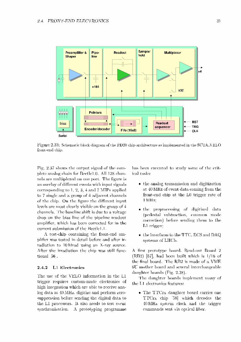
2.4. FRONT-END ELECTRONICS 31
Figure 2.33: Schematic block diagram of the RD20 chip architecture as implemented in the SCTA VELOfront-end chip.
Fig. 2.37 shows the output signal of the com-plete analog chain for Beetle1.0. All 128 chan-nels are multiplexed on one port. The gure isan overlay of dierent events with input signalscorresponding to 1, 2, 3, 4 and 7 MIPs appliedto 7 single and a group of 4 adjacent channelsof the chip. On the gure the dierent inputlevels are most clearly visible on the group of 4channels. The baseline shift is due to a voltagedrop on the bias line of the pipeline readoutamplier, which has been corrected for in thecurrent submission of the Beetle1.1.
A test-chip containing the front-end am-plier was tested in detail before and after ir-radiation to 10Mrad using an X-ray source.After the irradiation the chip was still func-tional [56].
2.4.2 L1 Electronics
The use of the VELO information in the L1trigger requires custom-made electronics ofhigh integration which are able to receive ana-log data at 40MHz, digitize and perform zero-suppression before sending the digital data tothe L1 processors. It also needs to test eventsynchronization. A prototyping programme
has been executed to study some of the crit-ical tasks:
the analog transmission and digitizationat 40MHz of event data coming from thefront-end chip at the L0 trigger rate of1MHz;
the preprocessing of digitized data(pedestal subtraction, common modecorrection) before sending them to theL1 trigger;
the interfaces to the TTC, ECS and DAQsystems of LHCb.
A rst prototype board, Read-out Board 2(RB2) [57], had been built which is 1/16 ofthe nal board. The RB2 is made of a VME6U mother board and several interchangeabledaughter boards (Fig. 2.38).
The daughter boards implement many ofthe L1 electronics features:
The TTCrx daughter board carries oneTTCrx chip [58] which decodes the40MHz system clock and the triggercommands sent via optical ber.
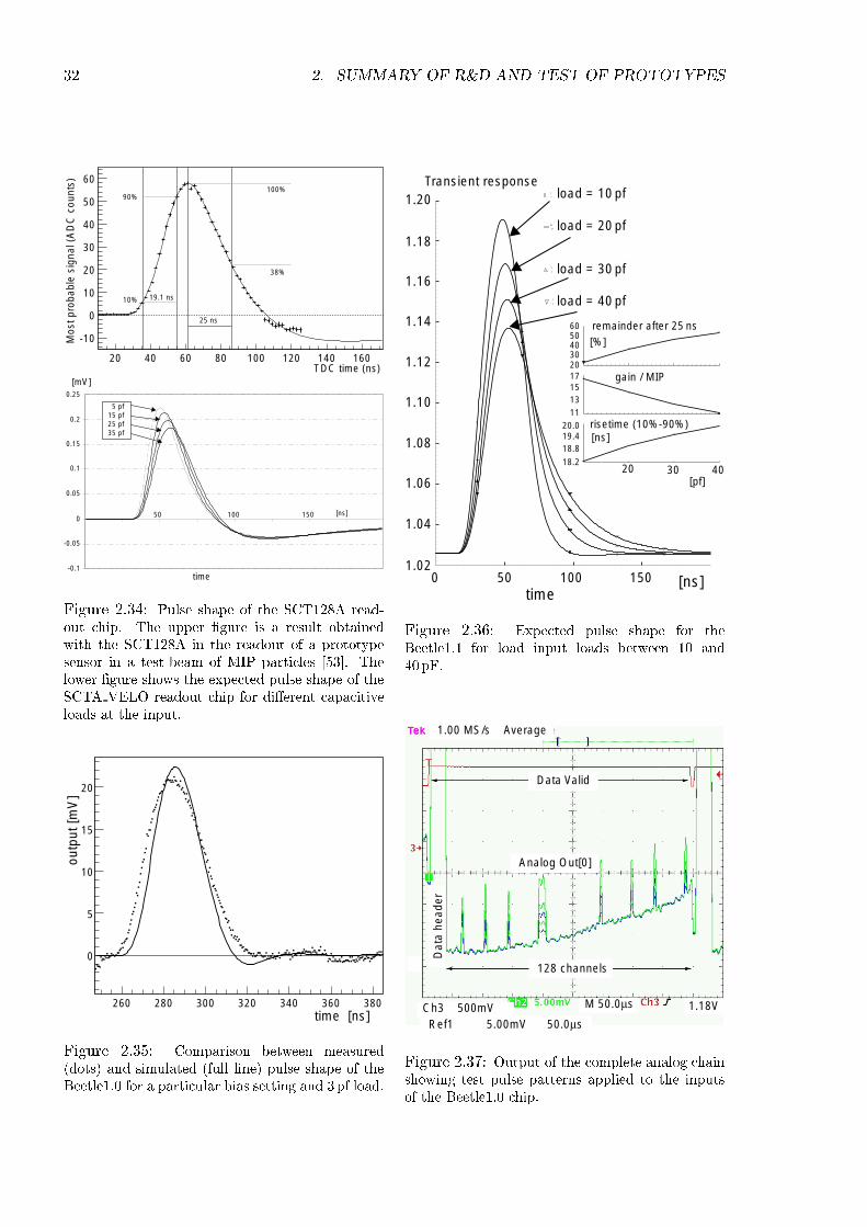
32 2. SUMMARY OF R&D AND TEST OF PROTOTYPES
TDC time (ns)20 40 60 80 100 120 140 160
Mos
t pro
babl
e si
gnal
(A
DC
cou
nts)
-10
0
10
20
30
40
50
60
25 ns
19.1 ns10%
90%100%
38%
0.25
0.2
0.1
-0.05
0.15
-0.1
0.05
0[ns]
time
10050 150
5 pf15 pf25 pf35 pf
[mV]
Figure 2.34: Pulse shape of the SCT128A read-out chip. The upper gure is a result obtainedwith the SCT128A in the readout of a prototypesensor in a test-beam of MIP particles [53]. Thelower gure shows the expected pulse shape of theSCTA VELO readout chip for dierent capacitiveloads at the input.
time [ns]260 280 300 320 340 360 380
outp
ut [m
V]
0
5
10
15
20
Figure 2.35: Comparison between measured(dots) and simulated (full line) pulse shape of theBeetle1.0 for a particular bias setting and 3pf load.
20 30 40[pf]
remainder after 25 ns
gain / MIP
risetime (10%-90%)
605040302017151311
20.019.418.8
18.2
[ns]
[%]
load = 10 pf
load = 20 pf
load = 30 pf
load = 40 pf
Transient response1.20
1.18
1.16
1.14
1.12
1.10
1.08
1.06
1.04
1.020 50 100 150
time[ns]
Figure 2.36: Expected pulse shape for theBeetle1.1 for load input loads between 10 and40pF.
Data Valid
128 channels
Analog Out[0]
1.00 MS/s Average
Ref1 5.00mV 50.0µsCh3 500mV M 50.0µs 1.18V
Dat
a he
ader
Figure 2.37: Output of the complete analog chainshowing test pulse patterns applied to the inputsof the Beetle1.0 chip.
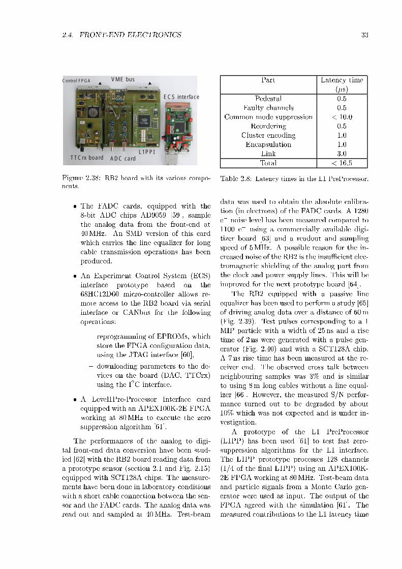
2.4. FRONT-END ELECTRONICS 33
ADC cardTTCrx board
ECS interface
VME busControl FPGA
L1PPI
Figure 2.38: RB2 board with its various compo-nents.
The FADC cards, equipped with the8-bit ADC chips AD9059 [59], samplethe analog data from the front-end at40MHz. An SMD version of this cardwhich carries the line equalizer for longcable transmission operations has beenproduced.
An Experiment Control System (ECS)interface prototype based on the68HC12D60 micro-controller allows re-mote access to the RB2 board via serialinterface or CANbus for the followingoperations:
reprogramming of EPROMs, whichstore the FPGA conguration data,using the JTAG interface [60],
downloading parameters to the de-vices on the board (DAC, TTCrx)using the I2C interface.
A Level1Pre-Processor Interface cardequipped with an APEX100K-2E FPGAworking at 80MHz to execute the zerosuppression algorithm [61].
The performances of the analog to digi-tal front-end data conversion have been stud-ied [62] with the RB2 board reading data froma prototype sensor (section 2.1 and Fig. 2.15)equipped with SCT128A chips. The measure-ments have been done in laboratory conditionswith a short cable connection between the sen-sor and the FADC cards. The analog data wasread out and sampled at 40MHz. Test-beam
Part Latency time(s)
Pedestal 0:5Faulty channels 0:5
Common mode suppression < 10:0Reordering 0:5
Cluster encoding 1:0Encapsulation 1:0
Link 3:0
Total < 16:5
Table 2.8: Latency times in the L1 PreProcessor.
data was used to obtain the absolute calibra-tion (in electrons) of the FADC cards. A 1280e noise level has been measured compared to1100 e using a commercially available digi-tizer board [63] and a readout and samplingspeed of 5MHz. A possible reason for the in-creased noise of the RB2 is the insuÆcient elec-tromagnetic shielding of the analog part fromthe clock and power supply lines. This will beimproved for the next prototype board [64].
The RB2 equipped with a passive lineequalizer has been used to perform a study [65]of driving analog data over a distance of 60m(Fig. 2.39). Test pulses corresponding to a 1MIP particle with a width of 25 ns and a risetime of 2 ns were generated with a pulse gen-erator (Fig. 2.40) and with a SCT128A chip.A 7 ns rise time has been measured at the re-ceiver end. The observed cross talk betweenneighbouring samples was 3% and is similarto using 8m long cables without a line equal-izer [66]. However, the measured S/N perfor-mance turned out to be degraded by about10% which was not expected and is under in-vestigation.
A prototype of the L1 PreProcessor(L1PP) has been used [61] to test fast zero-suppression algorithms for the L1 interface.The L1PP prototype processes 128 channels(1/4 of the nal L1PP) using an APEX100K-2E FPGA working at 80MHz. Test-beam dataand particle signals from a Monte Carlo gen-erator were used as input. The output of theFPGA agreed with the simulation [61]. Themeasured contributions to the L1 latency time
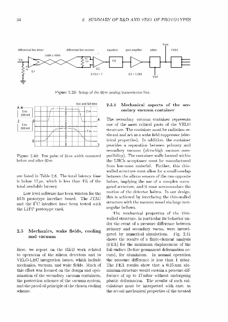
34 2. SUMMARY OF R&D AND TEST OF PROTOTYPES
R150
OPAMP2
-
+
R2120
differential line receiverdifferencial line driver
Vin
equalizer
cable L=60m
G1G2
G1G2 = 1
post amplifier adder FADC
Vref
Vout
G3 = 1,584
EQ
Figure 2.39: Setup of the 60m analog transmission line.
rise and fall time
7 ns
2 ns 5 ns200 mV
5 ns200 mV
A
2
2
A
0
0
Figure 2.40: Test pulse of 25 ns width measuredbefore and after 60m.
are listed in Table 2.8. The total latency timeis below 17s, which is less than 1% of thetotal available latency.
Low level software has been written for theECS prototype interface board. The JTAGand the I2C interface have been tested withthe L1PP prototype card.
2.5 Mechanics, wake elds, cooling
and vacuum
Here, we report on the R&D work relatedto operation of the silicon detectors and toVELO-LHC integration issues, which includemechanics, vacuum, and wake elds. Much ofthis eort was focused on the design and opti-mization of the secondary vacuum containers,the protection schemes of the vacuum system,and the proof-of-principle of the chosen coolingscheme.
2.5.1 Mechanical aspects of the sec-ondary vacuum container
The secondary vacuum container representsone of the most critical parts of the VELOstructure. The container must be radiation re-sistant and act as a wake eld suppressor (elec-trical properties). In addition, the containerprovides a separation between primary andsecondary vacuum (ultra-high vacuum com-patibility). The container walls located withinthe LHCb acceptance must be manufacturedfrom low-mass material. Further, this thin-walled structure must allow for a small overlapbetween the silicon sensors of the two oppositehalves, implying the use of a complex corru-gated structure, and it must accommodate themotion of the detector halves. In our design,this is achieved by interfacing the thin-walledstructure with the vacuum vessel via large rect-angular bellows.
The mechanical properties of the thin-walled structure, in particular its behavior un-der the event of a pressure dierence betweenprimary and secondary vacua, were investi-gated by numerical simulations. Fig. 2.41shows the results of a nite-element analysis(FEA) for the maximum displacement of thefoil surface (before permanent deformation oc-curs), for aluminium. In normal operationthe pressure dierence is less than 1 mbar.The FEA results show that a 0:25mm alu-minium structure would sustain a pressure dif-ference of up to 17mbar without undergoingplastic deformation. The results of such cal-culations must be interpreted with care, asthe actual mechanical properties of the treated
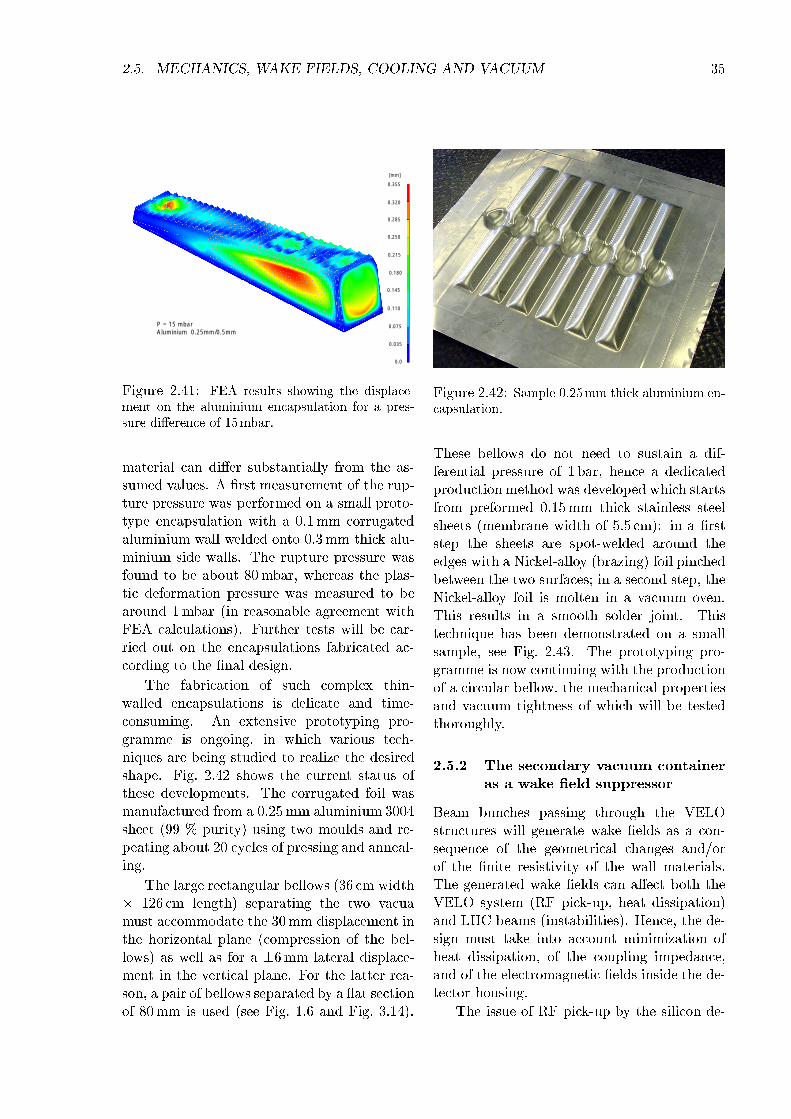
2.5. MECHANICS, WAKE FIELDS, COOLING AND VACUUM 35
P = 15 mbarAluminium 0.25mm/0.5mm
0.110
0.035
0.145
0.075
0.0
0.180
0.215
0.250
0.285
0.320
0.355
[mm]
Figure 2.41: FEA results showing the displace-ment on the aluminium encapsulation for a pres-sure dierence of 15mbar.
material can dier substantially from the as-sumed values. A rst measurement of the rup-ture pressure was performed on a small proto-type encapsulation with a 0:1mm corrugatedaluminium wall welded onto 0:3mm thick alu-minium side walls. The rupture pressure wasfound to be about 80mbar, whereas the plas-tic deformation pressure was measured to bearound 1mbar (in reasonable agreement withFEA calculations). Further tests will be car-ried out on the encapsulations fabricated ac-cording to the nal design.
The fabrication of such complex thin-walled encapsulations is delicate and time-consuming. An extensive prototyping pro-gramme is ongoing, in which various tech-niques are being studied to realize the desiredshape. Fig. 2.42 shows the current status ofthese developments. The corrugated foil wasmanufactured from a 0:25mm aluminium 3004sheet (99 % purity) using two moulds and re-peating about 20 cycles of pressing and anneal-ing.
The large rectangular bellows (36 cm width 126 cm length) separating the two vacuamust accommodate the 30mm displacement inthe horizontal plane (compression of the bel-lows) as well as for a 6mm lateral displace-ment in the vertical plane. For the latter rea-son, a pair of bellows separated by a at sectionof 80mm is used (see Fig. 1.6 and Fig. 3.14).
Figure 2.42: Sample 0:25mm thick aluminium en-capsulation.
These bellows do not need to sustain a dif-ferential pressure of 1 bar, hence a dedicatedproduction method was developed which startsfrom preformed 0:15mm thick stainless steelsheets (membrane width of 5:5 cm): in a rststep the sheets are spot-welded around theedges with a Nickel-alloy (brazing) foil pinchedbetween the two surfaces; in a second step, theNickel-alloy foil is molten in a vacuum oven.This results in a smooth solder joint. Thistechnique has been demonstrated on a smallsample, see Fig. 2.43. The prototyping pro-gramme is now continuing with the productionof a circular bellow, the mechanical propertiesand vacuum tightness of which will be testedthoroughly.
2.5.2 The secondary vacuum containeras a wake eld suppressor
Beam bunches passing through the VELOstructures will generate wake elds as a con-sequence of the geometrical changes and/orof the nite resistivity of the wall materials.The generated wake elds can aect both theVELO system (RF pick-up, heat dissipation)and LHC beams (instabilities). Hence, the de-sign must take into account minimization ofheat dissipation, of the coupling impedance,and of the electromagnetic elds inside the de-tector housing.
The issue of RF pick-up by the silicon de-
36 2. SUMMARY OF R&D AND TEST OF PROTOTYPES
Figure 2.43: Sample 0:15mm thick stainless steelmembrane manufactured according to the methoddescribed in the text.
tector modules was addressed by estimatingthe attenuation of the LHC electromagneticelds through the thin aluminium shield [67].The use of a 0:1mm thick aluminium foil,as proposed in the TP [1], might be insuf-cient to protect the detectors against high-frequency pick-up noise. Present calculationsyield a minimum thickness of 0:18mm. Pend-ing a more accurate determination based onmeasurements with a fully equipped detectormodule, the thickness has been increased to0.25mm.
We addressed the issues related to the lon-gitudinal loss factor and coupling impedanceby simulations with the codes MAFIA6 andABCI [68] which numerically solve Maxwell'sequations to obtain the wake elds. Calcula-tions in the frequency and time domain were
6MAFIA Collaboration, CST GmbH, Lautschlager-str 38, 64289 Darmstadt.
Figure 2.44: Photograph of a prototype wake eldsuppressor made of copper-beryllium alloy.
performed to study both resonant and tran-sient eects. In the design of the VELO,wake eld suppression is achieved by enclos-ing the silicon detector modules in a shieldingbox made of aluminium and ensuring that acontinuous conductive surface guides the mir-ror charges from one end of the VELO ves-sel to the other. The end connections con-sist of segmented half tapers fabricated from(19 cm long, 70 m thick) corrugated copper-beryllium strips (see Fig. 2.44 and Fig. 3.13).The corrugations are needed to allow for me-chanical motion of the detector housings rela-tive to the vacuum vessel and exit window.
In the LOI [69] and TP [1] designs the sili-con detector modules are individually enclosedin thin aluminium boxes which form a contin-uous wall structure with deep cavity-like cor-rugations. A rst study with MAFIA in thefrequency domain showed that such deep cor-
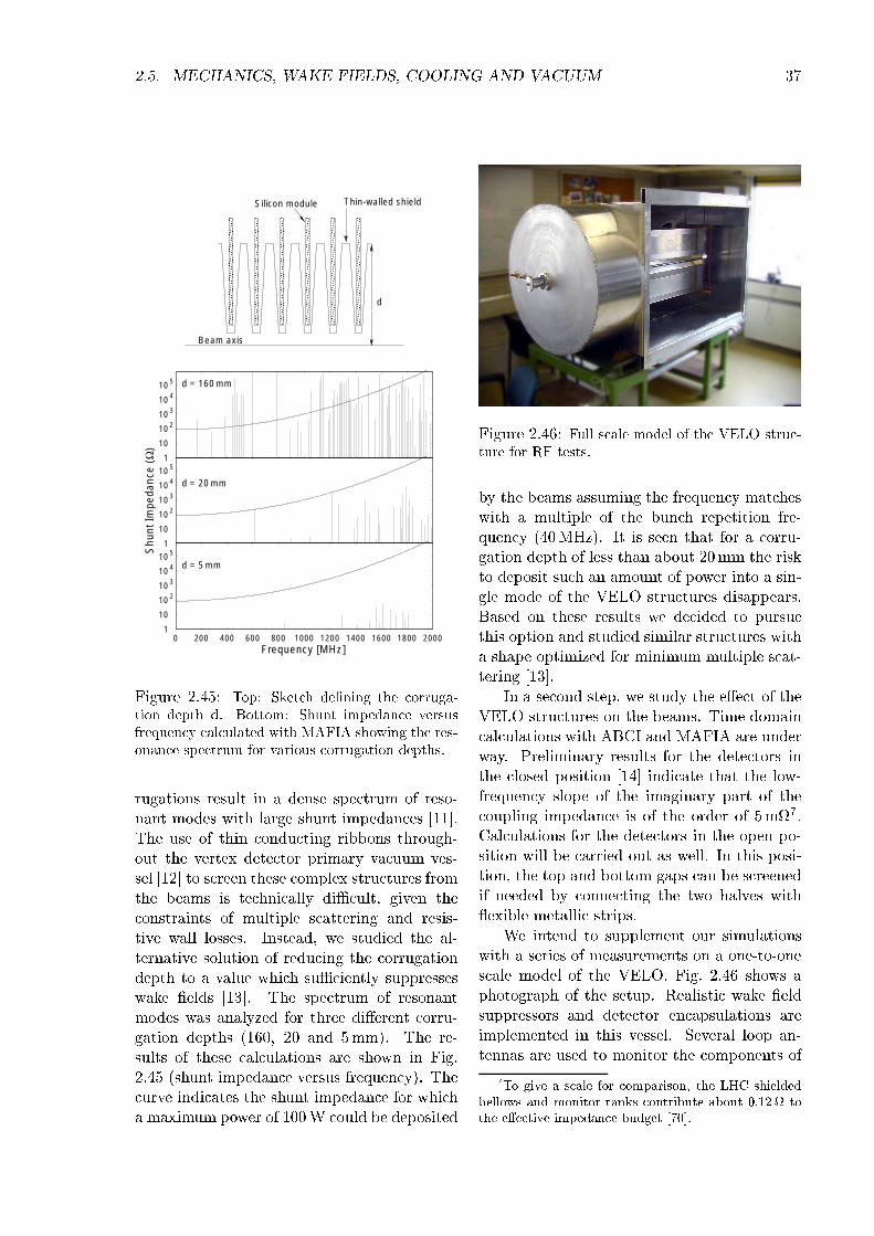
2.5. MECHANICS, WAKE FIELDS, COOLING AND VACUUM 37
d
Silicon module Thin-walled shield
Beam axis
Shu
nt Im
peda
nce
(Ω)
Frequency [MHz]
1
10
10 210 310 410 5
1
10
10 210 310 410 5
1
10
10 210 310 410 5
0 200 400 600 800 1000 1200 1400 1600 1800 2000
d = 160 mm
d = 20 mm
d = 5 mm
Figure 2.45: Top: Sketch dening the corruga-tion depth d. Bottom: Shunt impedance versusfrequency calculated with MAFIA showing the res-onance spectrum for various corrugation depths.
rugations result in a dense spectrum of reso-nant modes with large shunt impedances [11].The use of thin conducting ribbons through-out the vertex detector primary vacuum ves-sel [12] to screen these complex structures fromthe beams is technically diÆcult, given theconstraints of multiple scattering and resis-tive wall losses. Instead, we studied the al-ternative solution of reducing the corrugationdepth to a value which suÆciently suppresseswake elds [13]. The spectrum of resonantmodes was analyzed for three dierent corru-gation depths (160, 20 and 5mm). The re-sults of these calculations are shown in Fig.2.45 (shunt impedance versus frequency). Thecurve indicates the shunt impedance for whicha maximum power of 100W could be deposited
Figure 2.46: Full scale model of the VELO struc-ture for RF tests.
by the beams assuming the frequency matcheswith a multiple of the bunch repetition fre-quency (40MHz). It is seen that for a corru-gation depth of less than about 20mm the riskto deposit such an amount of power into a sin-gle mode of the VELO structures disappears.Based on these results we decided to pursuethis option and studied similar structures witha shape optimized for minimum multiple scat-tering [13].
In a second step, we study the eect of theVELO structures on the beams. Time domaincalculations with ABCI and MAFIA are underway. Preliminary results for the detectors inthe closed position [14] indicate that the low-frequency slope of the imaginary part of thecoupling impedance is of the order of 5m7.Calculations for the detectors in the open po-sition will be carried out as well. In this posi-tion, the top and bottom gaps can be screenedif needed by connecting the two halves with exible metallic strips.
We intend to supplement our simulationswith a series of measurements on a one-to-onescale model of the VELO. Fig. 2.46 shows aphotograph of the setup. Realistic wake eldsuppressors and detector encapsulations areimplemented in this vessel. Several loop an-tennas are used to monitor the components of
7To give a scale for comparison, the LHC shieldedbellows and monitor tanks contribute about 0:12 tothe eective impedance budget [70].
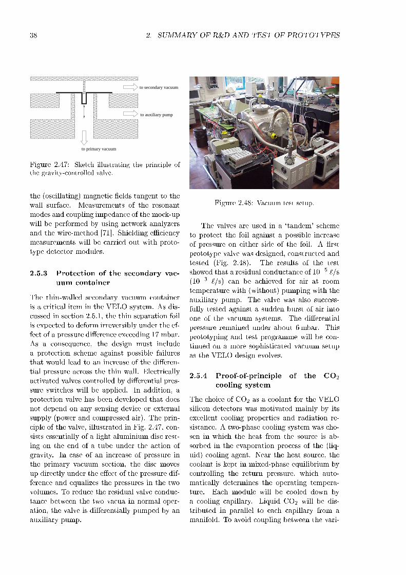
38 2. SUMMARY OF R&D AND TEST OF PROTOTYPES
to primary vacuum
to auxiliary pump
to secondary vacuum
Figure 2.47: Sketch illustrating the principle ofthe gravity-controlled valve.
the (oscillating) magnetic elds tangent to thewall surface. Measurements of the resonantmodes and coupling impedance of the mock-upwill be performed by using network analyzersand the wire-method [71]. Shielding eÆciencymeasurements will be carried out with proto-type detector modules.
2.5.3 Protection of the secondary vac-uum container
The thin-walled secondary vacuum containeris a critical item in the VELO system. As dis-cussed in section 2.5.1, the thin separation foilis expected to deform irreversibly under the ef-fect of a pressure dierence exceeding 17 mbar.As a consequence, the design must includea protection scheme against possible failuresthat would lead to an increase of the dieren-tial pressure across the thin wall. Electricallyactivated valves controlled by dierential pres-sure switches will be applied. In addition, aprotection valve has been developed that doesnot depend on any sensing device or externalsupply (power and compressed air). The prin-ciple of the valve, illustrated in Fig. 2.47, con-sists essentially of a light aluminium disc rest-ing on the end of a tube under the action ofgravity. In case of an increase of pressure inthe primary vacuum section, the disc movesup directly under the eect of the pressure dif-ference and equalizes the pressures in the twovolumes. To reduce the residual valve conduc-tance between the two vacua in normal oper-ation, the valve is dierentially pumped by anauxiliary pump.
Figure 2.48: Vacuum test setup.
The valves are used in a `tandem' schemeto protect the foil against a possible increaseof pressure on either side of the foil. A rstprototype valve was designed, constructed andtested (Fig. 2.48). The results of the testshowed that a residual conductance of 105 `/s(103 `/s) can be achieved for air at roomtemperature with (without) pumping with theauxiliary pump. The valve was also success-fully tested against a sudden burst of air intoone of the vacuum systems. The dierentialpressure remained under about 6mbar. Thisprototyping and test programme will be con-tinued on a more sophisticated vacuum setupas the VELO design evolves.
2.5.4 Proof-of-principle of the CO2
cooling system
The choice of CO2 as a coolant for the VELOsilicon detectors was motivated mainly by itsexcellent cooling properties and radiation re-sistance. A two-phase cooling system was cho-sen in which the heat from the source is ab-sorbed in the evaporation process of the (liq-uid) cooling agent. Near the heat source, thecoolant is kept in mixed-phase equilibrium bycontrolling the return pressure, which auto-matically determines the operating tempera-ture. Each module will be cooled down bya cooling capillary. Liquid CO2 will be dis-tributed in parallel to each capillary from amanifold. To avoid coupling between the vari-
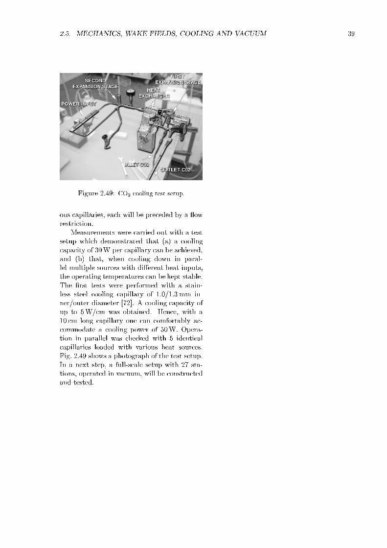
2.5. MECHANICS, WAKE FIELDS, COOLING AND VACUUM 39
Figure 2.49: CO2 cooling test setup.
ous capillaries, each will be preceded by a owrestriction.
Measurements were carried out with a testsetup which demonstrated that (a) a coolingcapacity of 30W per capillary can be achieved,and (b) that, when cooling down in paral-lel multiple sources with dierent heat inputs,the operating temperatures can be kept stable.The rst tests were performed with a stain-less steel cooling capillary of 1:0=1:3mm in-ner/outer diameter [72]. A cooling capacity ofup to 5W/cm was obtained. Hence, with a10 cm long capillary one can comfortably ac-commodate a cooling power of 50W. Opera-tion in parallel was checked with 5 identicalcapillaries loaded with various heat sources.Fig. 2.49 shows a photograph of the test setup.In a next step, a full-scale setup with 27 sta-tions, operated in vacuum, will be constructedand tested.

40 2. SUMMARY OF R&D AND TEST OF PROTOTYPES
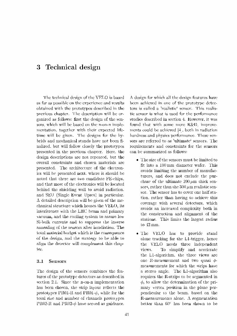
3 Technical design
The technical design of the VELO is basedas far as possible on the experience and resultsobtained with the prototypes described in theprevious chapter. The description will be or-ganized as follows: rst the design of the sen-sors, which will be based on the n-on-n imple-mentation, together with their expected life-time will be given. The designs for the hy-brids and mechanical stands have not been -nalized, but will follow closely the prototypespresented in the previous chapter. Here, thedesign descriptions are not repeated, but theoverall constraints and chosen materials arepresented. The architecture of the electron-ics will be presented next, where it should benoted that there are two candidate FE-chips,and that most of the electronics will be locatedbehind the shielding wall to avoid radiation,and SEU (Single Event Upset) in particular.A detailed description will be given of the me-chanical structure which houses the VELO, itsinterference with the LHC beam and primaryvacuum, and the cooling system to assure lowSi-bulk currents and to suppress the inverseannealing of the sensors after irradiation. Thetotal material budget which is the consequenceof the design, and the strategy to be able toalign the detector will complement this chap-ter.
3.1 Sensors
The design of the sensors combines the fea-tures of the prototype detectors as described insection 2.1. Since the n-on-n implementationhas been chosen, the strip layout re ects theprototypes PR01-R and PR01-, while for thetotal size and number of channels prototypesPR02-R and PR02- have served as guidance.
A design for which all the design features havebeen achieved in one of the prototype detec-tors is called a 'realistic` sensor. This realis-tic sensor is what is used for the performancestudies described in section 4. However, it wasfound that with some more R&D, improve-ments could be achieved [4], both in radiationhardness and physics performance. These sen-sors are referred to as 'ultimate` sensors. Therequirements and constraints for the sensorscan be summarized as follows:
The size of the sensors must be limited tot into a 100mm diameter wafer. Thisavoids limiting the number of manufac-turers, and does not exclude the pur-chase of the ultimate 200m thick sen-sors, rather than the 300m realistic sen-sor. The sensor has to cover one half sta-tion, rather than having to achieve thiscoverage with several detectors, whichavoids an increased complexity both inthe construction and alignment of thestations. This limits the largest radiusto 42mm.
The VELO has to provide standalone tracking for the L1-trigger, hencethe VELO needs three independentviews. To simplify and acceleratethe L1-algorithm, the three views areone R-measurement and two quasi -measurements for which the strips havea stereo angle. The L1-algorithm alsorequires the R-strips to be segmented in, to allow the determination of the pri-mary vertex position in the plane per-pendicular to the beam, based on theR-measurements alone. A segmentationbetter than 60Æ has been shown to be
41
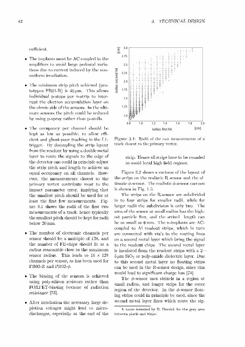
42 3. TECHNICAL DESIGN
suÆcient.
The implants must be AC coupled to theampliers to avoid large pedestal varia-tions due to current induced by the non-uniform irradiation.
The minimum strip pitch achieved (pro-totypes PR01-R) is 40m. This allowsindividual p-stops per n-strip to inter-rupt the electron accumulation layer onthe ohmic side of the sensors. In the ulti-mate sensors the pitch could be reducedby using p-spray rather than p-atolls.
The occupancy per channel should bekept as low as possible, to allow eÆ-cient and ghost-poor tracking in the L1-trigger. By decoupling the strip layoutfrom the readout by using a double metallayer to route the signals to the edge ofthe detector one could in principle adjustthe strip pitch and length to achieve anequal occupancy on all channels. How-ever, the measurements closest to theprimary vertex contribute most to theimpact parameter error, implying thatthe smallest pitch should be used for atleast the rst few measurements. Fig-ure 3.1 shows the radii of the rst twomeasurements of a track, hence typicallythe smallest pitch should be kept for radiibelow 20mm.
The number of electronic channels persensor should be a multiple of 128, andthe number of FE-chips should t at aradius reasonable close to the maximumsensor radius. This leads to 16 128channels per sensor, as has been used forPR02-R and PR02-.
The biasing of the sensors is achievedusing poly-silicon resistors rather thanFOXFET-biasing because of radiationresistance [73].
After irradiation the necessary large de-pletion voltages might lead to micro-discharges, especially at the end of the
radius first hit [cm]
0.8 1.0 1.2 1.4 1.6 1.8 2.0
1.25
1.0
1.5
1.75
2.0
2.25
2.5
2.75
3.0
radi
us s
econ
d hi
t[c
m]
Figure 3.1: Radii of the two measurements of atrack closest to the primary vertex.
strip. Hence all strips have to be roundedto avoid local high eld regions.
Figure 3.2 shows a cartoon of the layout ofthe strips on the realistic R-sensor and the ul-timate -sensor. The realistic -sensor cartoonis shown in Fig. 1.5.
The strips on the R-sensor are subdividedin to four strips for smaller radii, while forlarger radii the subdivision is only two. Thearea of the sensor at small radius has the high-est particle ux, and the strixel1 length canbe as small as 6mm. The n-implants are AC-coupled to Al readout strips, which in turnare connected with via's to the routing lineson a second metal layer which bring the signalto the readout chips. The second metal layeris insulated from the readout strips with a 25m SiO2 or poly-amide dielectric layer. Dueto this second metal layer no oating stripscan be used in the R-sensor design, since thiswould lead to signicant charge loss [74].
The -sensor uses strixels in a region atsmall radius, and longer strips for the outerregion of the detector. In the -sensor oat-ing strips could in principle be used, since thesecond metal layer lines which route the sig-
1A name invented by B. Henrich for the grey areabetween pixels and strips.
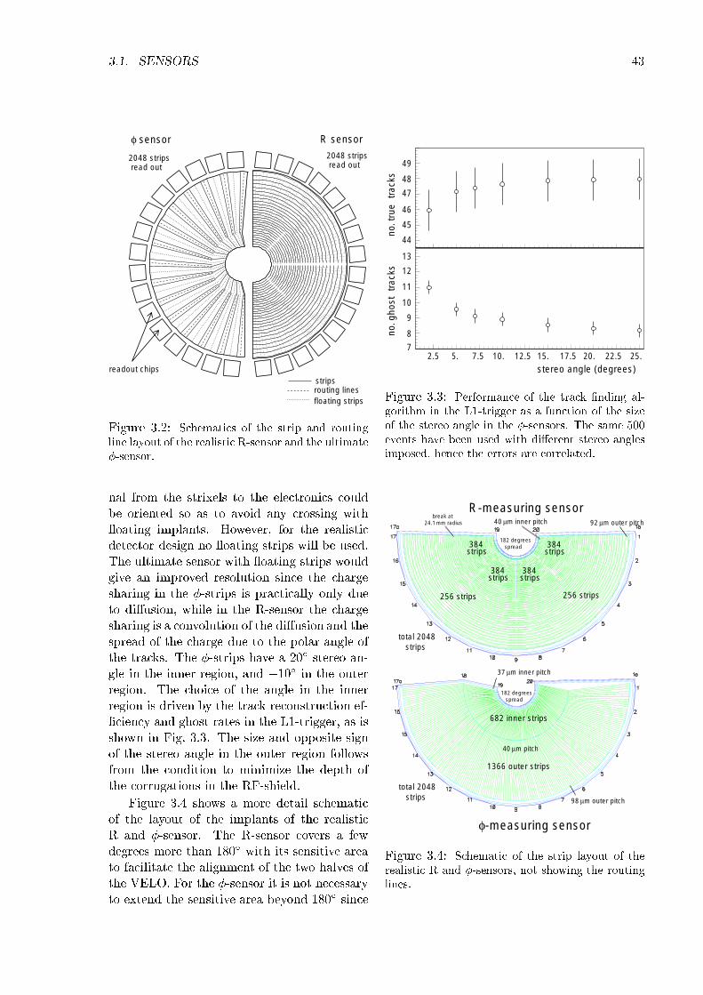
3.1. SENSORS 43
R sensor
stripsreadout chips
routing linesfloating strips
φ sensor
2048 strips read out
2048 strips read out
Figure 3.2: Schematics of the strip and routingline layout of the realistic R-sensor and the ultimate-sensor.
nal from the strixels to the electronics couldbe oriented so as to avoid any crossing with oating implants. However, for the realisticdetector design no oating strips will be used.The ultimate sensor with oating strips wouldgive an improved resolution since the chargesharing in the -strips is practically only dueto diusion, while in the R-sensor the chargesharing is a convolution of the diusion and thespread of the charge due to the polar angle ofthe tracks. The -strips have a 20Æ stereo an-gle in the inner region, and 10Æ in the outerregion. The choice of the angle in the innerregion is driven by the track reconstruction ef-ciency and ghost rates in the L1-trigger, as isshown in Fig. 3.3. The size and opposite signof the stereo angle in the outer region followsfrom the condition to minimize the depth ofthe corrugations in the RF-shield.
Figure 3.4 shows a more detail schematicof the layout of the implants of the realisticR and -sensor. The R-sensor covers a fewdegrees more than 180Æ with its sensitive areato facilitate the alignment of the two halves ofthe VELO. For the -sensor it is not necessaryto extend the sensitive area beyond 180Æ since
stereo angle (degrees)
no. t
rue
trac
ksno
. gho
st t
rack
s
2.5 5. 7.5 10. 12.5 15. 17.5 20. 22.5 25.7
47
46
45
44
13
12
11
10
9
8
48
49
Figure 3.3: Performance of the track nding al-gorithm in the L1-trigger as a function of the sizeof the stereo angle in the -sensors. The same 500events have been used with dierent stereo anglesimposed, hence the errors are correlated.
φ-measuring sensor
R-measuring sensor
40 µm pitch
37 µm inner pitch
182 degrees spread
682 inner strips
1366 outer strips
384 strips
384 strips
384 strips
384 strips
256 strips 256 strips
92 µm outer pitch40 µm inner pitch
182 degrees spread
break at24.1 mm radius
98 µm outer pitch
total 2048 strips
total 2048 strips
Figure 3.4: Schematic of the strip layout of therealistic R and -sensors, not showing the routinglines.
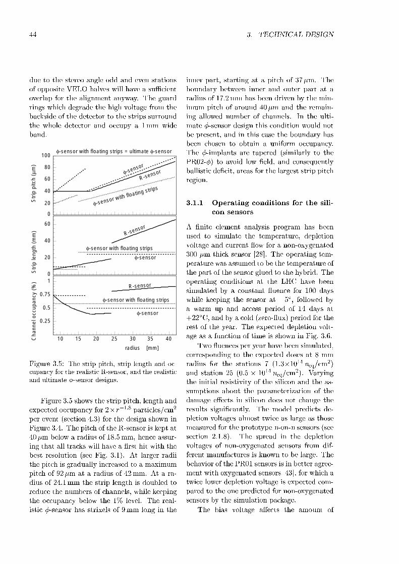
44 3. TECHNICAL DESIGN
due to the stereo angle odd and even stationsof opposite VELO halves will have a suÆcientoverlap for the alignment anyway. The guardrings which degrade the high voltage from thebackside of the detector to the strips surroundthe whole detector and occupy a 1mm wideband.
φ-sensor with floating strips = ultimate φ-sensor
φ-sensor
φ-sensor with floating strips
φ-sensor with floating strips
φ-sensor with floating strips
R-sensor
φ-sensor
φ-sensor
R-sensor
R-sensor
Cha
nnel
occ
upan
cy (
%)
Str
ip le
ngth
(m
m)
Str
ip p
itch
(µm
)
100
80
60
40
20
0
60
40
20
01
0.75
0.5
0.25
10 15 20 25 30 35 40
radius [mm]
Figure 3.5: The strip pitch, strip length and oc-cupancy for the realistic R-sensor, and the realisticand ultimate -sensor designs.
Figure 3.5 shows the strip pitch, length andexpected occupancy for 2r1:8 particles/cm2
per event (section 4.3) for the design shown inFigure 3.4. The pitch of the R-sensor is kept at40m below a radius of 18:5mm, hence assur-ing that all tracks will have a rst hit with thebest resolution (see Fig. 3.1). At larger radiithe pitch is gradually increased to a maximumpitch of 92m at a radius of 42mm. At a ra-dius of 24:1mm the strip length is doubled toreduce the numbers of channels, while keepingthe occupancy below the 1% level. The real-istic -sensor has strixels of 9mm long in the
inner part, starting at a pitch of 37m. Theboundary between inner and outer part at aradius of 17:2mm has been driven by the min-imum pitch of around 40m and the remain-ing allowed number of channels. In the ulti-mate -sensor design this condition would notbe present, and in this case the boundary hasbeen chosen to obtain a uniform occupancy.The -implants are tapered (similarly to thePR02-) to avoid low eld, and consequentlyballistic decit, areas for the largest strip pitchregion.
3.1.1 Operating conditions for the sili-con sensors
A nite element analysis program has beenused to simulate the temperature, depletionvoltage and current ow for a non-oxygenated300 m thick sensor [28]. The operating tem-perature was assumed to be the temperature ofthe part of the sensor glued to the hybrid. Theoperating conditions at the LHC have beensimulated by a constant uence for 100 dayswhile keeping the sensor at 5Æ, followed bya warm up and access period of 14 days at+22ÆC, and by a cold (zero- ux) period for therest of the year. The expected depletion volt-age as a function of time is shown in Fig. 3.6.
Two uences per year have been simulated,corresponding to the expected doses at 8 mmradius for the stations 7 (1.31014 neq/cm2)and station 25 (0:5 1014 neq/cm
2). Varyingthe initial resistivity of the silicon and the as-sumptions about the parameterization of thedamage eects in silicon does not change theresults signicantly. The model predicts de-pletion voltages almost twice as large as thosemeasured for the prototype n-on-n sensors (seesection 2.1.8). The spread in the depletionvoltages of non-oxygenated sensors from dif-ferent manufactures is known to be large. Thebehavior of the PR01 sensors is in better agree-ment with oxygenated sensors [43], for which atwice lower depletion voltage is expected com-pared to the one predicted for non-oxygenatedsensors by the simulation package.
The bias voltage aects the amount of
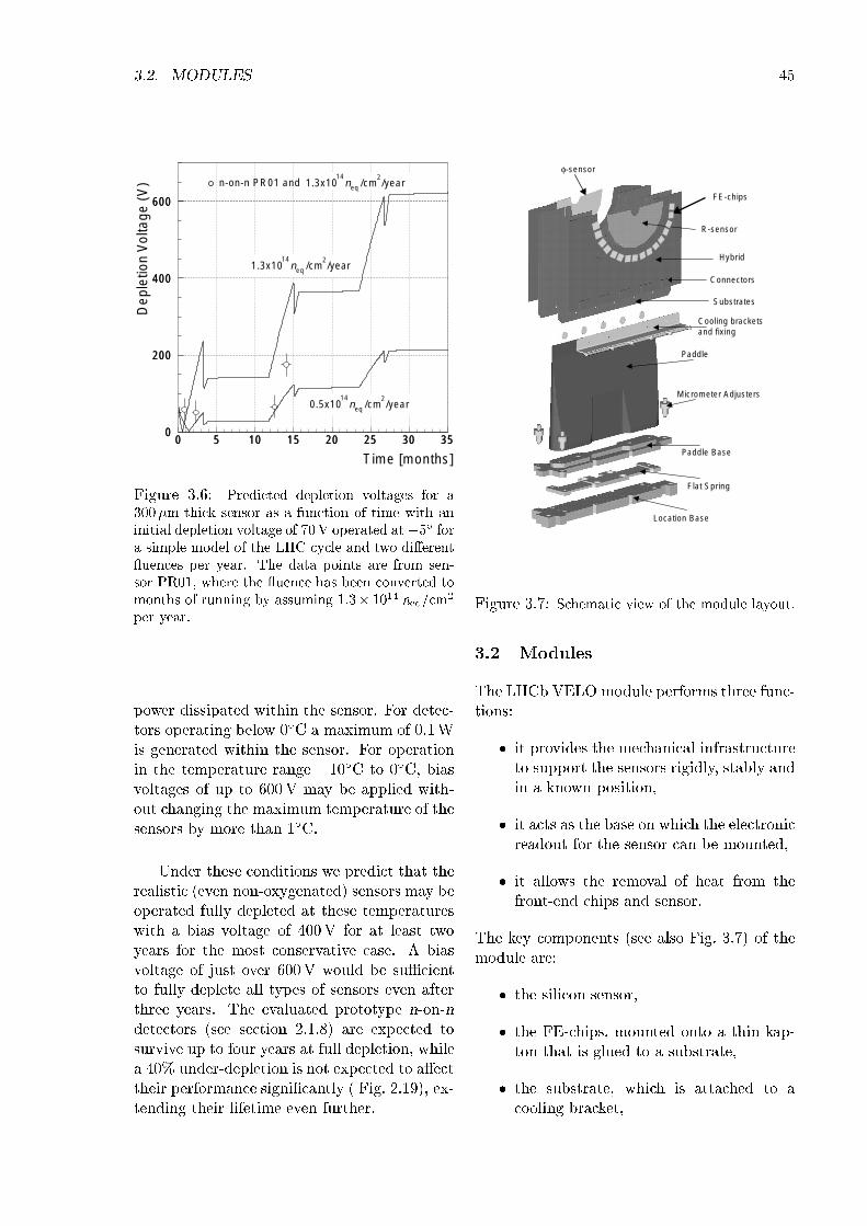
3.2. MODULES 45
0
200
400
600
0 5 10 15 20 25 30 350
200
400
600
0 5 10 15 20 25 30 35
n-on-n PR01 and 14 2
Time [months]
Dep
letio
n V
olta
ge (
V)
1.3x10 n /cm /year14 2
eq
0.5x10 n /cm /year14 2
eq
1.3x10 n /cm /year14 2
eq
Figure 3.6: Predicted depletion voltages for a300m thick sensor as a function of time with aninitial depletion voltage of 70V operated at 5Æ fora simple model of the LHC cycle and two dierent uences per year. The data points are from sen-sor PR01, where the uence has been converted tomonths of running by assuming 1:3 1014 neq/cm
2
per year.
power dissipated within the sensor. For detec-tors operating below 0ÆC a maximum of 0:1Wis generated within the sensor. For operationin the temperature range 10ÆC to 0ÆC, biasvoltages of up to 600 V may be applied with-out changing the maximum temperature of thesensors by more than 1ÆC.
Under these conditions we predict that therealistic (even non-oxygenated) sensors may beoperated fully depleted at these temperatureswith a bias voltage of 400V for at least twoyears for the most conservative case. A biasvoltage of just over 600V would be suÆcientto fully deplete all types of sensors even afterthree years. The evaluated prototype n-on-ndetectors (see section 2.1.8) are expected tosurvive up to four years at full depletion, whilea 40% under-depletion is not expected to aecttheir performance signicantly ( Fig. 2.19), ex-tending their lifetime even further.
Hybrid
Substrates
Cooling bracketsand fixing
Paddle
Micrometer Adjusters
Paddle Base
Flat Spring
φ-sensor
R-sensor
Location Base
FE-chips
Connectors
Figure 3.7: Schematic view of the module layout.
3.2 Modules
The LHCb VELO module performs three func-tions:
it provides the mechanical infrastructureto support the sensors rigidly, stably andin a known position,
it acts as the base on which the electronicreadout for the sensor can be mounted,
it allows the removal of heat from thefront-end chips and sensor.
The key components (see also Fig. 3.7) of themodule are:
the silicon sensor,
the FE-chips, mounted onto a thin kap-ton that is glued to a substrate,
the substrate, which is attached to acooling bracket,
46 3. TECHNICAL DESIGN
the substrate assembly, which is mountedonto a low mass carbon bre paddle thatseparates the sensors from the platform,
the paddle, attached onto a paddle basemade of aluminium. The base is con-nected via a at spring to a location base.
A summary of the material used in themodule is given in Table 3.1.
The module is designed to allow the pre-cision alignment of the sensors relative to theplatform on which all modules are mounted.This is made possible by the incorporation ofprecisely machined location surfaces into themodule (on the location base). The sensors canbe moved in 3 directions (x, y, z) and rotatedabout three axes relative to the location sur-faces. During the assembly the paddle is rstglued to the paddle base and then the heightand tilt of the sensors are adjusted with the mi-crometer screws relative to the location base.
3.3 Front-end electronics
3.3.1 System architecture
The key components of the front-end electron-ics architecture are shown in Fig. 3.8. Onesilicon sensor is read out by 16 front-end chipsmounted on one hybrid. Five repeater cardsper hybrid are mounted directly on the out-side of the vacuum tank. Four cards drive theanalog signals over twisted pair cables to thedigitizer boards in the counting room at a dis-tance of 60m. One other repeater card receivesthe timing and control signals and the low volt-age for the front-end chips as well as the biasvoltage for the sensor. All analog data of onesensor are received and processed by one digi-tizer board. The low voltage and high voltagepower supplies are situated behind the shield-ing wall in a radiation safe environment. Theelectronics can be divided into L0 electronics(front-end chips, hybrids) and L1 electronics(analog links, digitizer boards).
3.3.2 L0 Electronics
The L0 electronics deal with data before theL0 decision.
Front-end chip
A front-end chip for LHCb has to sample de-tector information with the LHC bunch cross-ing frequency of 40MHz. The data have to bestored in the chip for the 4s latency of the L0trigger decision. In order to ensure safe opera-tion of the VELO, the decision has been takento store analog information, which allows themonitoring of pedestals and noise on a chan-nel by channel basis and to subtract commonmode noise in the digitizer boards as part ofthe hit nding algorithm. The most importantdesign parameters for the chip are listed in Ta-ble 3.2 (for more details see Ref. [76]). The re-quirement about the tolerable signal left overafter 25 ns (pulse spill-over) is derived from astudy of the L1 trigger eÆciency. If the sig-nals left over are too high, the L1 trigger startsto reconstruct tracks from the previous bunchcrossing and assign them a large impact pa-rameter. The output of the L1 trigger willthen be saturated by fake b-events. It had beenshown [17, 77], that the trigger eÆciency is notaected by a spill-over of less than 30%. With30% spill-over, the number of clusters increasesby (2 3)%.
Two front-end chip candidates(SCTA VELO and Beetle) will be describedin this section. The nal decision which chipto adopt for the VELO at the startup of theLHC will be taken in March 2002 at the latestafter testing the functionality of both chipsbefore and after irradiation.
SCTA VELO: The SCTA VELO front-endchip (Fig. 2.33) is derived from the SCT128Adesign [31] with the following main modica-tions:
The pipeline is extended to 184 cells in-cluding 16 cells of de-randomizing buer,in order to accommodate a latency of4s.
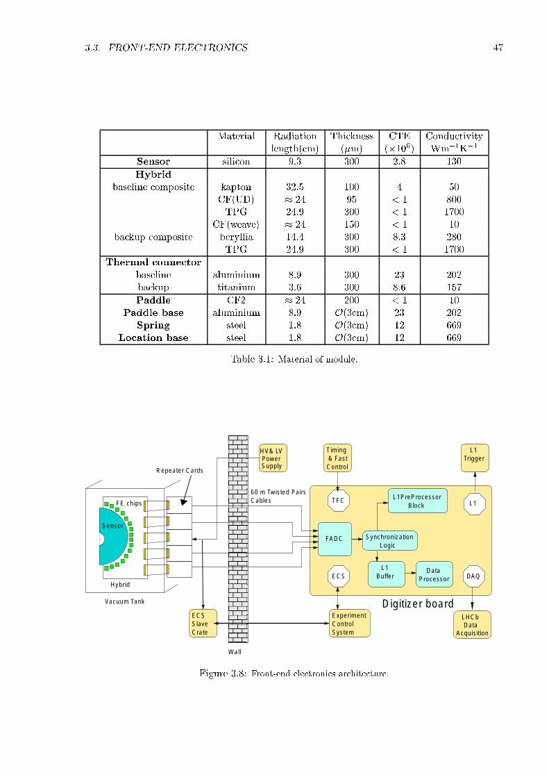
3.3. FRONT-END ELECTRONICS 47
Material Radiation Thickness CTE Conductivitylength(cm) (m) (106) Wm1K1
Sensor silicon 9:3 300 2:8 130
Hybridbaseline composite kapton 32:5 100 4 50
CF(UD) 24 95 < 1 800TPG 24:9 300 < 1 1700
CF(weave) 24 150 < 1 10backup composite beryllia 14:4 300 8:3 280
TPG 24:9 300 < 1 1700
Thermal connectorbaseline aluminium 8:9 300 23 202backup titanium 3:6 300 8:6 157
Paddle CF2 24 200 < 1 10Paddle base aluminium 8:9 O(3cm) 23 202
Spring steel 1:8 O(3cm) 12 669Location base steel 1:8 O(3cm) 12 669
Table 3.1: Material of module.
Sensor
FE chips
Hybrid
Vacuum Tank
ECSSlaveCrate
LHCb DataAcquisition
ExperimentControlSystem
Wall
Repeater Cards
PowerSupply
HV& LV Timing & FastControl
L1Trigger
TFC
DAQ
L1
ECS
FADC SynchronizationLogic
L1PreProcessorBlock
L1Buffer
DataProcessor
Digitizer board
60 m Twisted PairsCables
Figure 3.8: Front-end electronics architecture.
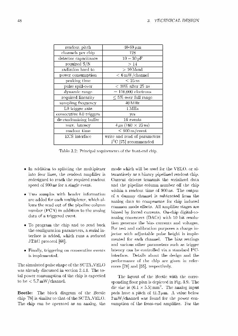
48 3. TECHNICAL DESIGN
readout pitch 40-60 m
channels per chip 128
detector capacitance 10 30 pF
required S/N > 14
radiation hard to > 10Mrad
power consumption < 6mW/channel
peaking time 25 ns
pulse spill-over < 30% after 25 ns
dynamic range 110,000 electrons
required linearity 5% over full range
sampling frequency 40MHz
L0 trigger rate 1MHz
consecutive L0 triggers yes
de-randomizing buer 16 events
max. latency 4s (160 25 ns)
readout time 900 ns/event
ECS interface write and read of parametersI2C [75] recommended
Table 3.2: Principal requirements of the front-end chip.
In addition to splitting the multiplexerinto four lines, the readout amplier isredesigned to reach the required readoutspeed of 900 ns for a single event.
Two samples with header informationare added for each multiplexer, which al-lows the read out of the pipeline columnnumber (PCN) in addition to the analogdata of a triggered event.
To program the chip and to read backthe conguration parameters, a serial in-terface is added, which runs a reducedJTAG protocol [60].
Finally, triggering on consecutive eventsis implemented.
The simulated pulse shape of the SCTA VELOwas already discussed in section 2.4.1. The to-tal power consumption of the chip is expectedto be < 5:7mW/channel.
Beetle: The block diagram of the Beetlechip [78] is similar to that of the SCTA VELO.The chip can be operated as an analog, the
mode which will be used for the VELO, or al-ternatively as a binary pipelined readout chip.Current drivers transmit the serialized dataand the pipeline column number o the chipwithin a readout time of 900 ns. The outputof a dummy channel is subtracted from theanalog data to compensate for chip inducedcommon mode eects. All amplier stages arebiased by forced currents. On-chip digital-to-analog converters (DACs) with 10 bit resolu-tion generate the bias currents and voltages.For test and calibration purposes a charge in-jector with adjustable pulse height is imple-mented for each channel. The bias settingsand various other parameters such as triggerlatency can be controlled via a standard I2C-interface. Details about the design and theperformance of the chip are given in refer-ences [78] and [55], respectively.
The layout of the Beetle with the corre-sponding oor plan is depicted in Fig. 3.9. Thedie size is (6:1 5:5)mm2. The analog inputpads have a pitch of 41:2m. A value below2mW/channel was found for the power con-sumption of the front-end amplier. For the
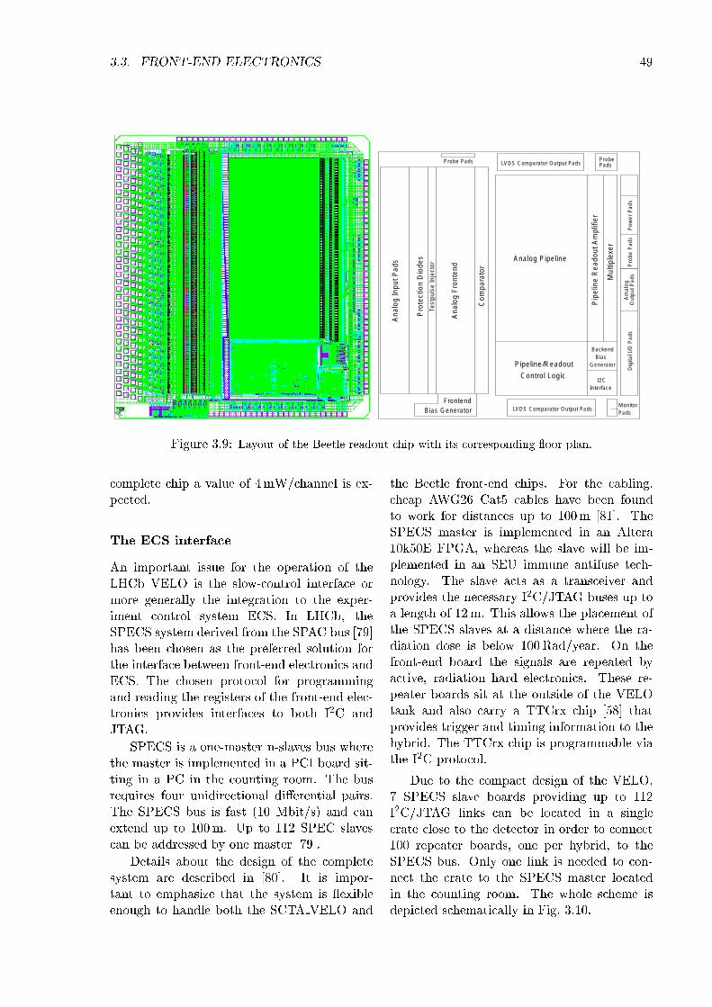
3.3. FRONT-END ELECTRONICS 49
Pipeline/Readout
Control LogicI2C
BackendBias
Generator
InterfaceA
nalo
g In
put P
ads
Pro
tect
ion
Dio
des
Test
puls
e In
ject
or
Ana
log
Fron
tend
Com
para
tor
Bias GeneratorFrontend
Pip
elin
e R
eado
ut A
mpl
ifier
Mul
tiple
xer
Analog Pipeline
Probe Pads
PadsMonitor
LVDS Comparator Output Pads
LVDS Comparator Output Pads PadsProbe
Pow
er P
ads
Pro
be P
ads
Am
alog
Out
put P
ads
Dig
ital I
/O P
ads
Figure 3.9: Layout of the Beetle readout chip with its corresponding oor plan.
complete chip a value of 4mW/channel is ex-pected.
The ECS interface
An important issue for the operation of theLHCb VELO is the slow-control interface ormore generally the integration to the exper-iment control system ECS. In LHCb, theSPECS system derived from the SPAC bus [79]has been chosen as the preferred solution forthe interface between front-end electronics andECS. The chosen protocol for programmingand reading the registers of the front-end elec-tronics provides interfaces to both I2C andJTAG.
SPECS is a one-master n-slaves bus wherethe master is implemented in a PCI board sit-ting in a PC in the counting room. The busrequires four unidirectional dierential pairs.The SPECS bus is fast (10 Mbit/s) and canextend up to 100m. Up to 112 SPEC slavescan be addressed by one master [79].
Details about the design of the completesystem are described in [80]. It is impor-tant to emphasize that the system is exibleenough to handle both the SCTA VELO and
the Beetle front-end chips. For the cabling,cheap AWG26 Cat5 cables have been foundto work for distances up to 100m [81]. TheSPECS master is implemented in an Altera10k50E FPGA, whereas the slave will be im-plemented in an SEU immune antifuse tech-nology. The slave acts as a transceiver andprovides the necessary I2C/JTAG buses up toa length of 12m. This allows the placement ofthe SPECS slaves at a distance where the ra-diation dose is below 100 Rad/year. On thefront-end board the signals are repeated byactive, radiation hard electronics. These re-peater boards sit at the outside of the VELOtank and also carry a TTCrx chip [58] thatprovides trigger and timing information to thehybrid. The TTCrx chip is programmable viathe I2C protocol.
Due to the compact design of the VELO,7 SPECS slave boards providing up to 112I2C/JTAG links can be located in a singlecrate close to the detector in order to connect100 repeater boards, one per hybrid, to theSPECS bus. Only one link is needed to con-nect the crate to the SPECS master locatedin the counting room. The whole scheme isdepicted schematically in Fig. 3.10.
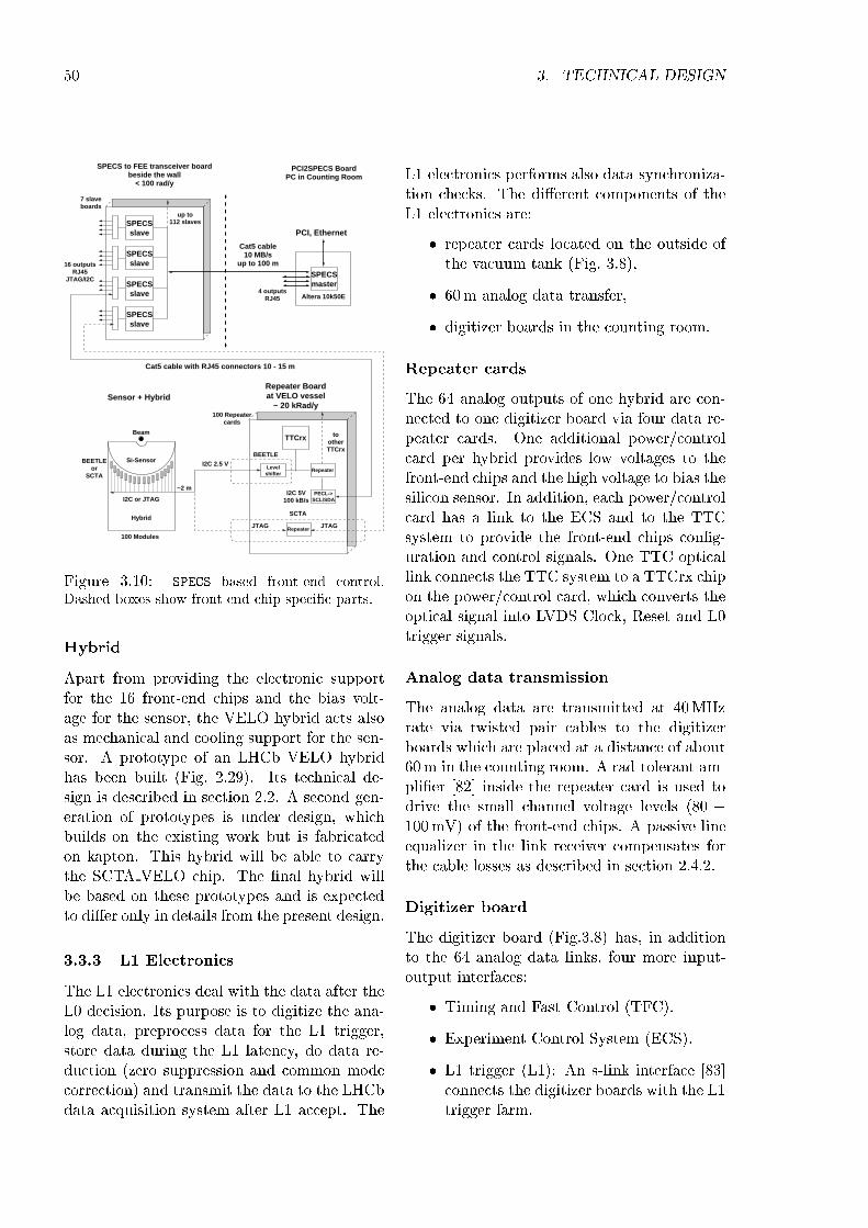
50 3. TECHNICAL DESIGN
Cat5 cable10 MB/s
up to 100 m
up to112 slaves
16 outputsRJ45
JTAG/I2C
4 outputsRJ45
BEETLEor
SCTA
Repeater
TTCrx
Levelshifter
Repeater
PECL->SCL/SDA
Repeater Boardat VELO vessel
~ 20 kRad/y
tootherTTCrx
100 Repeatercards
7 slaveboards
I2C 5V100 kB/s
beside the wall< 100 rad/y
SPECS to FEE transceiver board
masterSPECS
slaveSPECS
SPECSslave
SPECSslave
SPECSslave
PCI2SPECS BoardPC in Counting Room
BEETLE
SCTA
JTAG JTAG
I2C 2.5 V
Beam
Si-Sensor
Sensor + Hybrid
Cat5 cable with RJ45 connectors 10 - 15 m
Altera 10k50E
PCI, Ethernet
I2C or JTAG
Hybrid
100 Modules
~2 m
Figure 3.10: SPECS based front-end control.Dashed boxes show front-end chip specic parts.
Hybrid
Apart from providing the electronic supportfor the 16 front-end chips and the bias volt-age for the sensor, the VELO hybrid acts alsoas mechanical and cooling support for the sen-sor. A prototype of an LHCb VELO hybridhas been built (Fig. 2.29). Its technical de-sign is described in section 2.2. A second gen-eration of prototypes is under design, whichbuilds on the existing work but is fabricatedon kapton. This hybrid will be able to carrythe SCTA VELO chip. The nal hybrid willbe based on these prototypes and is expectedto dier only in details from the present design.
3.3.3 L1 Electronics
The L1 electronics deal with the data after theL0 decision. Its purpose is to digitize the ana-log data, preprocess data for the L1 trigger,store data during the L1 latency, do data re-duction (zero suppression and common modecorrection) and transmit the data to the LHCbdata acquisition system after L1 accept. The
L1 electronics performs also data synchroniza-tion checks. The dierent components of theL1 electronics are:
repeater cards located on the outside ofthe vacuum tank (Fig. 3.8),
60m analog data transfer,
digitizer boards in the counting room.
Repeater cards
The 64 analog outputs of one hybrid are con-nected to one digitizer board via four data re-peater cards. One additional power/controlcard per hybrid provides low voltages to thefront-end chips and the high voltage to bias thesilicon sensor. In addition, each power/controlcard has a link to the ECS and to the TTCsystem to provide the front-end chips cong-uration and control signals. One TTC opticallink connects the TTC system to a TTCrx chipon the power/control card, which converts theoptical signal into LVDS Clock, Reset and L0trigger signals.
Analog data transmission
The analog data are transmitted at 40MHzrate via twisted pair cables to the digitizerboards which are placed at a distance of about60m in the counting room. A rad-tolerant am-plier [82] inside the repeater card is used todrive the small channel voltage levels (80 100mV) of the front-end chips. A passive lineequalizer in the link receiver compensates forthe cable losses as described in section 2.4.2.
Digitizer board
The digitizer board (Fig.3.8) has, in additionto the 64 analog data links, four more input-output interfaces:
Timing and Fast Control (TFC).
Experiment Control System (ECS).
L1 trigger (L1): An s-link interface [83]connects the digitizer boards with the L1trigger farm.
3.3. FRONT-END ELECTRONICS 51
Data AcQuisition (DAQ): An s-link in-terface that connects the digitizer boardto the LHCb data acquisition system.
The Link Receivers digitize the analog dataat a frequency of 40MHz. The Synchroniza-tion Logic groups the event data coming viafour analog links from each front-end chip. Theevent data are copied to the L1 PreProces-sor (L1PP) and stored at the same time inthe L1 buer until the L1 accept/reject sig-nal is issued. The L1PP performs event datareduction and sends clusters to the L1 trig-ger. The Data Processor removes the rejectedevents from the L1 buers and processes theaccepted events in order to create clusters tobe sent out to the DAQ.
Link Receiver and SynchronizationLogic: The Link Receiver consists of a lineequalizer, an amplier and an FADC. Fouranalog data streams, corresponding to theoutput of one front-end chip, are fed into fourFIFO's controlled by one FPGA. To checksynchronization, the 8-bit Pipeline ControlNumber (PCN) coming with the front-endchip data is compared with the PCN providedby an emulator. In case of on error the eventis agged accordingly.
L1 PreProcessor, L1 buer and DataProcessor: Each of the four L1 PreProces-sor blocks processes the data of four front-end chips (= 512 channels). The data arestored in an input FIFO. A local memorywhich is loaded via ECS contains the pedestaland threshold values for every channel. Faultychannels can be masked. Data are correctedfor common mode noise and a cluster ndingalgorithm is executed based on the thresholdinformation. The clusters are stored into anoutput FIFO, which holds a maximum of 128clusters. The L1 interface receives the clus-ters from the four output FIFO's, packs themtogether according to the format proposed inthe L1 Trigger requirements document [84], en-capsulates them according to the s-link proto-col [85] and sends the event to the Read-out
Units of the L1 trigger. Events with more than128 clusters per digitizer board are agged andthe additional clusters are ignored.
The same data that are sent to the L1 Pre-Processor are also copied to the L1 buer wait-ing for the L1 decision. The L1 buer holdsup to ' 1900 events and is implemented as oneDMA memory of 512 kbyte for 8 input links.
After a positive L1 decision, the data aretransferred from the L1 buer to the L1 de-randomizer buer2, where they remain untilthe data processor is ready to accept the nextevent. The output of the data processor is keptin the Output Buer until it is transferred tothe LHCb data acquisition system.
The Data Processor performs a similardata reduction as the L1PP but with a bet-ter precision and lower thresholds since it hasabout a factor 10 more time available. TheData Processor runs also a L1PP emulator pro-cess that allows to record in an LHCb event theinput which was sent to the L1 trigger. A smallfraction of the event data are recorded withoutzero-suppression for oine monitoring of thepedestals and noise per strip.
The processing is done by DSPs3 with aprocessing power of 2000MIPS. Each DSP pro-cesses data from 8 input links. The L1 deran-domizer buer and the Output Buer are im-plemented using the DSP internal data mem-ory of 64 kbytes: 8 kbytes are used to imple-ment a 32-event deep L1 derandomizer buer;the remaining 56 kbytes are used to implementthe Output Buer. A cluster is coded using 6to 12 bytes in the output data format: 4 bytesfor the cluster address and L1 information and2 to 8 bytes with the individual strip chargevalues. The average event size in the outputbuer (assuming an average 1% occupancy) is15 bytes per DSP, which corresponds to a totalsize of 12 kbytes per event for the full VELO.The maximum L1 accepted event size in theOutput Buer is 512 bytes: therefore in theworst possible case the Output Buer is able
2http://lhcb-elec.web.cern.ch/lhcb-elec/html /ar-chitecture.htm
3TMS320C620X DSP Texas Instruments,http://dspvillage.ti.com/docs/dspproducthome.jhtml
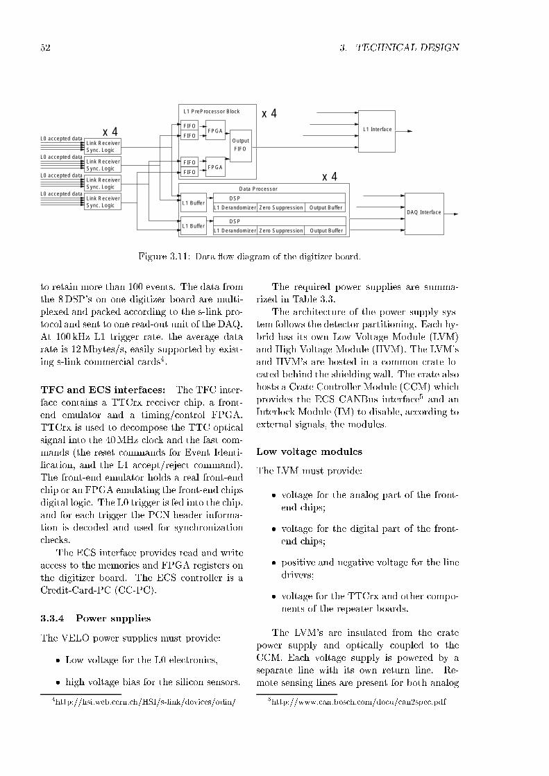
52 3. TECHNICAL DESIGN
L1 Buffer
L1 Buffer
DSP
L1 Derandomizer Zero Suppression Output Buffer
DSP
L1 Derandomizer Zero Suppression Output Buffer
L0 accepted dataLink ReceiverSync. Logic
L0 accepted dataLink ReceiverSync. Logic
L0 accepted dataLink ReceiverSync. Logic
L0 accepted dataLink ReceiverSync. Logic
FIFO
FIFO
L1 Interface
DAQ Interface
x 4
x 4
x 4FIFO
Output
L1 PreProcessor Block
FPGA
FPGAFIFO
FIFO
Data Processor
Figure 3.11: Data ow diagram of the digitizer board.
to retain more than 100 events. The data fromthe 8DSP's on one digitizer board are multi-plexed and packed according to the s-link pro-tocol and sent to one read-out unit of the DAQ.At 100 kHz L1 trigger rate, the average datarate is 12Mbytes/s, easily supported by exist-ing s-link commercial cards4.
TFC and ECS interfaces: The TFC inter-face contains a TTCrx receiver chip, a front-end emulator and a timing/control FPGA.TTCrx is used to decompose the TTC opticalsignal into the 40MHz clock and the fast com-mands (the reset commands for Event Identi-cation, and the L1 accept/reject command).The front-end emulator holds a real front-endchip or an FPGA emulating the front-end chipsdigital logic. The L0 trigger is fed into the chip,and for each trigger the PCN header informa-tion is decoded and used for synchronizationchecks.
The ECS interface provides read and writeaccess to the memories and FPGA registers onthe digitizer board. The ECS controller is aCredit-Card-PC (CC-PC).
3.3.4 Power supplies
The VELO power supplies must provide:
Low voltage for the L0 electronics,
high voltage bias for the silicon sensors.
4http://hsi.web.cern.ch/HSI/s-link/devices/odin/
The required power supplies are summa-rized in Table 3.3.
The architecture of the power supply sys-tem follows the detector partitioning. Each hy-brid has its own Low Voltage Module (LVM)and High Voltage Module (HVM). The LVM'sand HVM's are hosted in a common crate lo-cated behind the shielding wall. The crate alsohosts a Crate Controller Module (CCM) whichprovides the ECS CANBus interface5 and anInterlock Module (IM) to disable, according toexternal signals, the modules.
Low voltage modules
The LVM must provide:
voltage for the analog part of the front-end chips;
voltage for the digital part of the front-end chips;
positive and negative voltage for the linedrivers;
voltage for the TTCrx and other compo-nents of the repeater boards.
The LVM's are insulated from the cratepower supply and optically coupled to theCCM. Each voltage supply is powered by aseparate line with its own return line. Re-mote sensing lines are present for both analog
5http://www.can.bosch.com/docu/can2spec.pdf
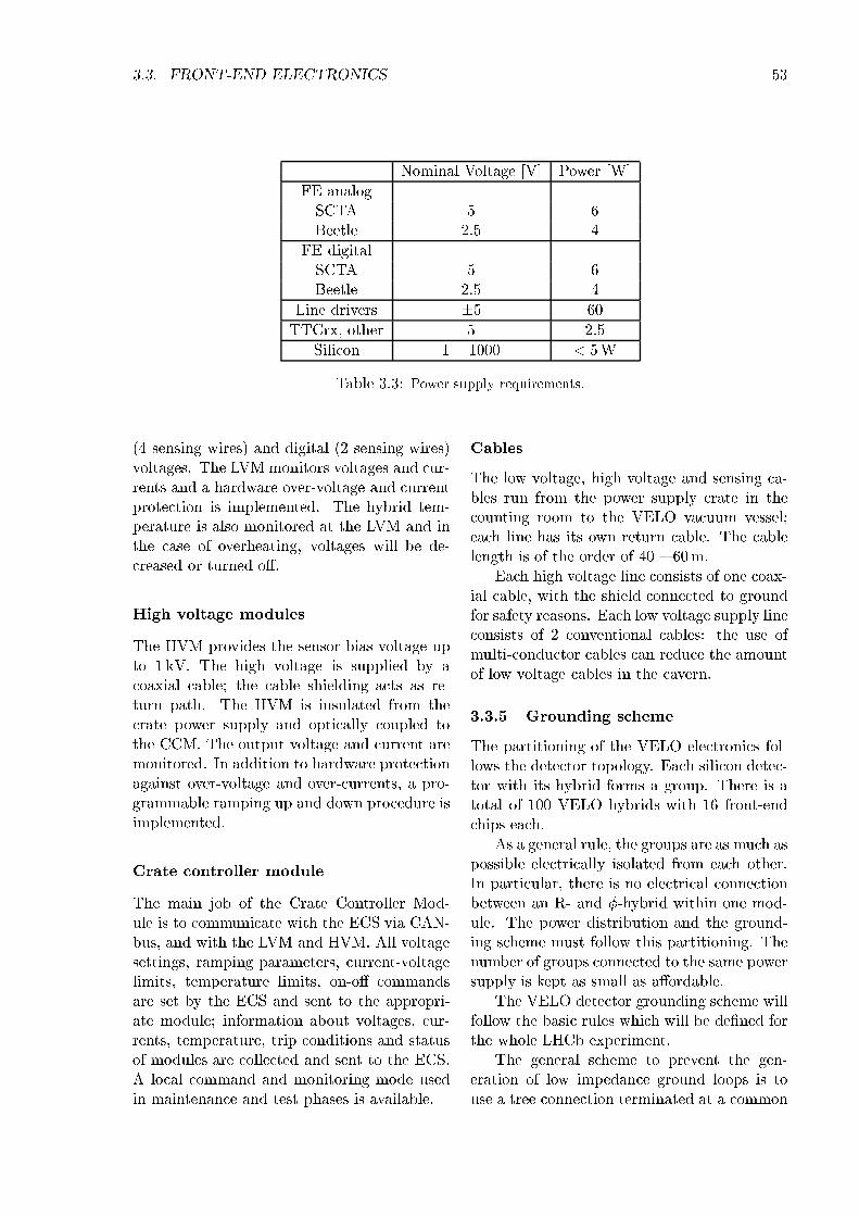
3.3. FRONT-END ELECTRONICS 53
Nominal Voltage [V] Power [W]
FE analogSCTA 5 6Beetle 2:5 4
FE digitalSCTA 5 6Beetle 2:5 4
Line drivers 5 60
TTCrx, other 5 2:5
Silicon 1 1000 < 5W
Table 3.3: Power supply requirements.
(4 sensing wires) and digital (2 sensing wires)voltages. The LVM monitors voltages and cur-rents and a hardware over-voltage and currentprotection is implemented. The hybrid tem-perature is also monitored at the LVM and inthe case of overheating, voltages will be de-creased or turned o.
High voltage modules
The HVM provides the sensor bias voltage upto 1 kV. The high voltage is supplied by acoaxial cable; the cable shielding acts as re-turn path. The HVM is insulated from thecrate power supply and optically coupled tothe CCM. The output voltage and current aremonitored. In addition to hardware protectionagainst over-voltage and over-currents, a pro-grammable ramping up and down procedure isimplemented.
Crate controller module
The main job of the Crate Controller Mod-ule is to communicate with the ECS via CAN-bus, and with the LVM and HVM. All voltagesettings, ramping parameters, current-voltagelimits, temperature limits, on-o commandsare set by the ECS and sent to the appropri-ate module; information about voltages, cur-rents, temperature, trip conditions and statusof modules are collected and sent to the ECS.A local command and monitoring mode usedin maintenance and test phases is available.
Cables
The low voltage, high voltage and sensing ca-bles run from the power supply crate in thecounting room to the VELO vacuum vessel;each line has its own return cable. The cablelength is of the order of 40 60m.
Each high voltage line consists of one coax-ial cable, with the shield connected to groundfor safety reasons. Each low voltage supply lineconsists of 2 conventional cables: the use ofmulti-conductor cables can reduce the amountof low voltage cables in the cavern.
3.3.5 Grounding scheme
The partitioning of the VELO electronics fol-lows the detector topology. Each silicon detec-tor with its hybrid forms a group. There is atotal of 100 VELO hybrids with 16 front-endchips each.
As a general rule, the groups are as much aspossible electrically isolated from each other.In particular, there is no electrical connectionbetween an R- and -hybrid within one mod-ule. The power distribution and the ground-ing scheme must follow this partitioning. Thenumber of groups connected to the same powersupply is kept as small as aordable.
The VELO detector grounding scheme willfollow the basic rules which will be dened forthe whole LHCb experiment.
The general scheme to prevent the gen-eration of low impedance ground loops is touse a tree connection terminated at a common
54 3. TECHNICAL DESIGN
grounding point. The VELO detector treegrounding scheme will have the common pointlocated on the hybrid side and will follow thepartitioning described above. When required,capacitors and/or resistors will be used to de-couple on and o detector electronics. We givea short description of the implementation forthe relevant subsystems.
Low voltage power supplies: The lowvoltage power supplies (less than 50V)are grounded at the hybrid side (seeSafety connection).
High voltage power supplies: Therange of voltages required is below 1 kV.The VELO uses a coaxial cable with theshield connected to ground at the powersupply side for safety reasons. The HVpower supply is grounded via an appro-priate resistor at the detector side.
Safety connection: The safety pointlocation for LHCb in the cavern will bedened mid-2001. All the VELO me-chanics parts such as the vacuum system,cooling system and RF shield, are con-nected to the beam pipe. The groundpoint must never be interrupted. Thefollowing options have been identied:
connection of the hybrids to groundvia the cooling pipes
connection via the mechanical hy-brid support
connection to a point outside of thetank, using an extra line.
The nal choice will be done after an insitu optimization, which will attempt toreduce the electronic noise that may beinduced by this connection.
Signal links: All the analog data andthe control lines use shielded twistedpairs. The shield of the cable is con-nected to the repeater card ground and isdecoupled by a capacitor at the digitizerboard.
3.4 Mechanics
The mechanical structure that houses the sil-icon detectors (more details can be found inRef. [8]) diers considerably from the one de-scribed in the Technical Proposal [1], in par-ticular with respect to the vacuum envelope,detector support frames and xy-table.
Firstly, requirements are listed, imposed byboth the LHC machine and the LHCb exper-iment, which the design of the vacuum vesseland support structures of the vertex locatorneed to meet.
LHC requirements:
Beam-induced bombardment inside thevacuum vessel must be low enough thateects on the beam lifetime and stabilityare kept at an acceptable level [86].
During data taking the silicon detectorsare placed at 8 mm from the circulat-ing protons. However, during injectionthe required half aperture amounts to27mm [87]. The complete silicon detec-tor array and encapsulations must be re-tractable such that no material remainswithin this radius during beam injectionand ramping.
The VELO should not degrade the LHCbeam conditions by parasitic RF cou-pling.
No LHCb-specic failure scenario shouldlead to an (expected) downtime for theLHC that exceeds two weeks.
LHCb requirements:
The acceptance of the vertex detectorwill be 300mrad 250mrad (horizontal vertical). Multiple scattering in thevacuum envelope, wake eld suppressorsand exit window should be kept to a min-imum. The geometry should be such asto be compatible with subsequent detec-tors (e.g. T1 and RICH1).
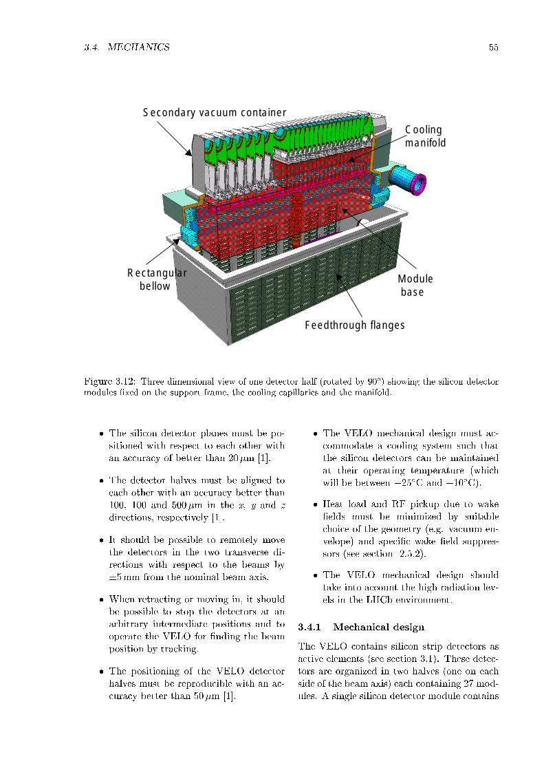
3.4. MECHANICS 55
Secondary vacuum container
Coolingmanifold
Feedthrough flanges
Rectangular bellow
Module base
Figure 3.12: Three dimensional view of one detector half (rotated by 90Æ) showing the silicon detectormodules xed on the support frame, the cooling capillaries and the manifold.
The silicon detector planes must be po-sitioned with respect to each other withan accuracy of better than 20m [1].
The detector halves must be aligned toeach other with an accuracy better than100, 100 and 500m in the x, y and zdirections, respectively [1].
It should be possible to remotely movethe detectors in the two transverse di-rections with respect to the beams by5mm from the nominal beam axis.
When retracting or moving in, it shouldbe possible to stop the detectors at anarbitrary intermediate positions and tooperate the VELO for nding the beamposition by tracking.
The positioning of the VELO detectorhalves must be reproducible with an ac-curacy better than 50m [1].
The VELO mechanical design must ac-commodate a cooling system such thatthe silicon detectors can be maintainedat their operating temperature (whichwill be between 25ÆC and +10ÆC).
Heat load and RF pickup due to wakeelds must be minimized by suitablechoice of the geometry (e.g. vacuum en-velope) and specic wake eld suppres-sors (see section 2.5.2).
The VELO mechanical design shouldtake into account the high radiation lev-els in the LHCb environment.
3.4.1 Mechanical design
The VELO contains silicon strip detectors asactive elements (see section 3.1). These detec-tors are organized in two halves (one on eachside of the beam axis) each containing 27 mod-ules. A single silicon detector module contains
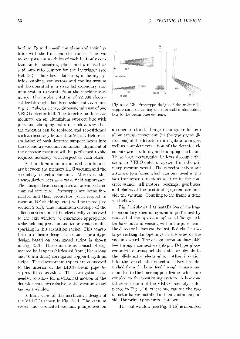
56 3. TECHNICAL DESIGN
both an R- and a -silicon plane and their hy-brids with the front-end electronics. The twomost upstream modules of each half only con-tain an R-measuring plane and are used asa pile-up veto counter for the L0 trigger (seeRef. [3]). The silicon detectors, including hy-brids, cabling, connectors and cooling systemwill be operated in a so-called secondary vac-uum system (separate from the machine vac-uum). The implementation of 22; 000 electri-cal feedthroughs has been taken into account.Fig. 3.12 shows a three dimensional view of oneVELO detector half. The detector modules aremounted on an aluminium support box withpins and clamping bolts in such a way thatthe modules can be replaced and repositionedwith an accuracy better than 20m. Before in-stallation of both detector support boxes intothe secondary vacuum containers, alignment ofthe detector modules will be performed to therequired accuracy with respect to each other.
A thin aluminium box is used as a bound-ary between the primary LHC vacuum and thesecondary detector vacuum. Moreover, thisencapsulation acts as a wake eld suppressor.The encapsulation comprises an advanced me-chanical structure. Prototypes are being fab-ricated and their properties (with respect tovacuum, RF shielding, etc.) will be tested (seesection 2.5.1). The aluminium envelope of thesilicon stations must be electrically connectedto the exit window to guarantee appropriatewake eld suppression and to prevent possiblesparking in this transition region. This consti-tutes a delicate design issue and a prototypedesign based on corrugated strips is shownin Fig. 3.13. The connections consist of seg-mented half tapers fabricated from (19 cm longand 70 m thick) corrugated copper-berylliumstrips. The downstream tapers are connectedto the interior of the LHCb beam pipe bya press-t connection. The corrugations areneeded to allow for mechanical motion of thedetector housings relative to the vacuum vesseland exit window.
A front view of the mechanical design ofthe VELO is shown in Fig. 3.14. The vacuumvessel and associated vacuum pumps rest on
TOP
FRONT
194 RIGHT
222
11.6
14
56
ISO
exit window
Figure 3.13: Prototype design of the wake eldsuppressors connecting the thin-walled aluminiumbox to the beam pipe sections.
a concrete stand. Large rectangular bellowsallow precise movement (in the transverse di-rections) of the detectors during data taking aswell as complete retraction of the detector el-ements prior to lling and dumping the beam.These large rectangular bellows decouple thecomplete VELO detector system from the pri-mary vacuum vessel. The detector halves areattached to a frame which can be moved in thetwo transverse directions relative to the con-crete stand. All motors, bearings, gearboxesand chains of the positioning system are out-side the vacuum. Coupling to the frame is donevia bellows.
Fig. 3.15 shows that installation of the frag-ile secondary vacuum system is performed byremoval of the upstream spherical ange. Af-ter bake out and venting with ultra-pure neon,the detector halves can be installed via the twolarge rectangular openings in the sides of thevacuum vessel. The design accommodates 440feedthrough connectors (50-pin D-type glass-ceramic) to transport the detector signals tothe o-detector electronics. After insertioninto the vessel, the detector halves are de-tached from the large feedthrough anges andmounted to the inner support frames which arecoupled to the positioning system. A horizon-tal cross section of the VELO assembly is de-picted in Fig. 3.16, where one can see the twodetector halves installed in their containers, in-side the primary vacuum chamber.
The exit window (see Fig. 3.16) is mounted
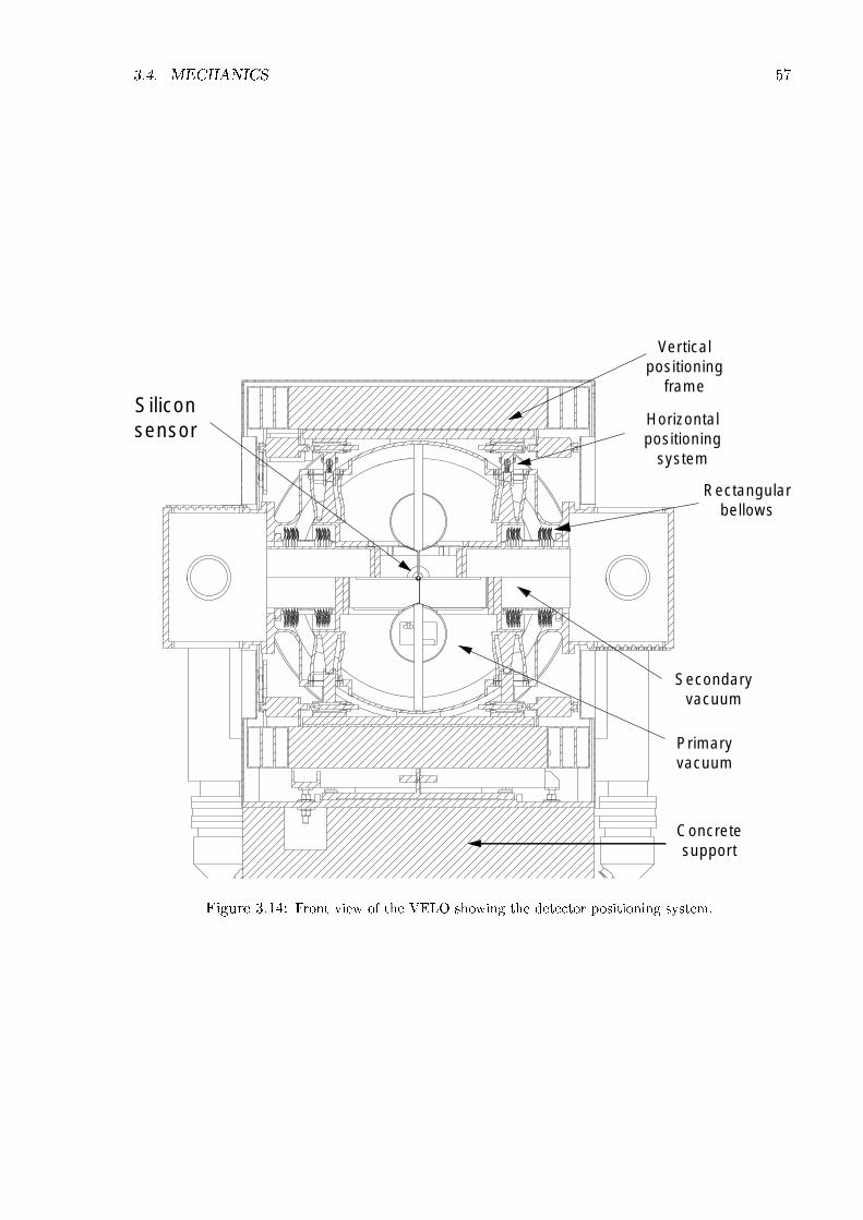
3.4. MECHANICS 57
Siliconsensor
Verticalpositioning
frame
Horizontalpositioning
system
Rectangularbellows
Secondaryvacuum
Primaryvacuum
Concretesupport
Figure 3.14: Front view of the VELO showing the detector positioning system.
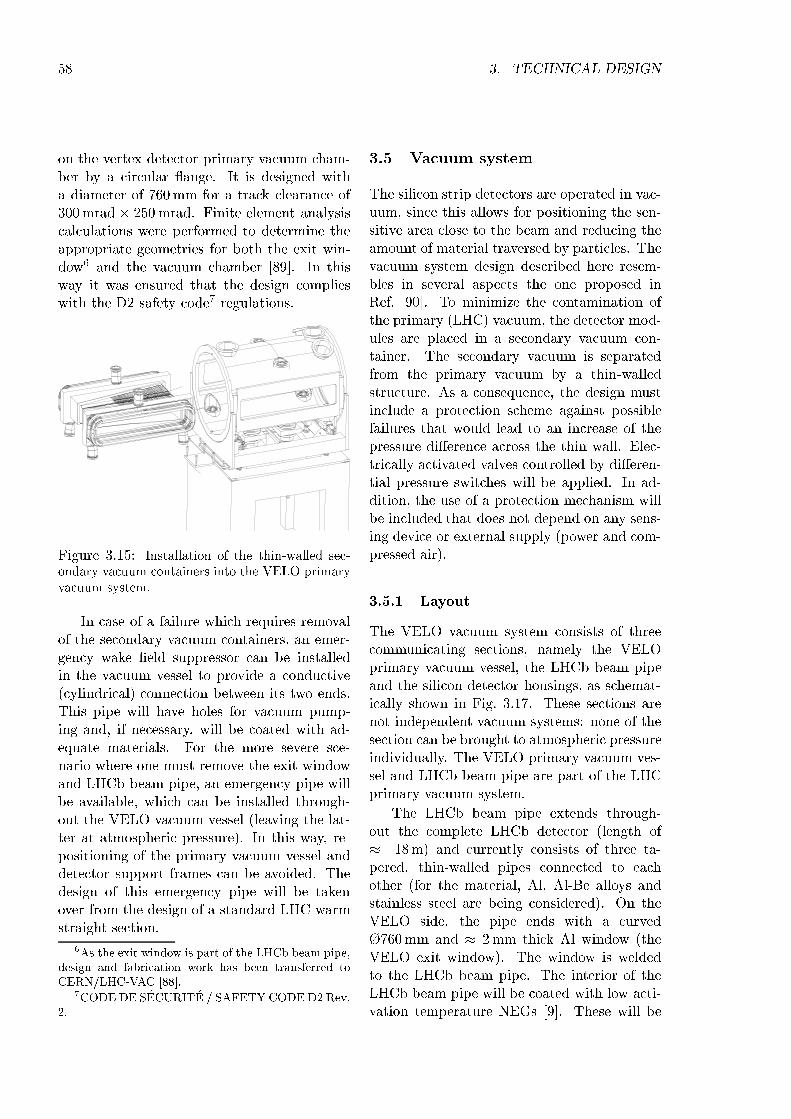
58 3. TECHNICAL DESIGN
on the vertex detector primary vacuum cham-ber by a circular ange. It is designed witha diameter of 760mm for a track clearance of300mrad 250mrad. Finite element analysiscalculations were performed to determine theappropriate geometries for both the exit win-dow6 and the vacuum chamber [89]. In thisway it was ensured that the design complieswith the D2 safety code7 regulations.
Figure 3.15: Installation of the thin-walled sec-ondary vacuum containers into the VELO primaryvacuum system.
In case of a failure which requires removalof the secondary vacuum containers, an emer-gency wake eld suppressor can be installedin the vacuum vessel to provide a conductive(cylindrical) connection between its two ends.This pipe will have holes for vacuum pump-ing and, if necessary, will be coated with ad-equate materials. For the more severe sce-nario where one must remove the exit windowand LHCb beam pipe, an emergency pipe willbe available, which can be installed through-out the VELO vacuum vessel (leaving the lat-ter at atmospheric pressure). In this way, re-positioning of the primary vacuum vessel anddetector support frames can be avoided. Thedesign of this emergency pipe will be takenover from the design of a standard LHC warmstraight section.
6As the exit window is part of the LHCb beam pipe,design and fabrication work has been transferred toCERN/LHC-VAC [88].
7CODE DE SECURITE / SAFETY CODE D2 Rev.2.
3.5 Vacuum system
The silicon strip detectors are operated in vac-uum, since this allows for positioning the sen-sitive area close to the beam and reducing theamount of material traversed by particles. Thevacuum system design described here resem-bles in several aspects the one proposed inRef. [90]. To minimize the contamination ofthe primary (LHC) vacuum, the detector mod-ules are placed in a secondary vacuum con-tainer. The secondary vacuum is separatedfrom the primary vacuum by a thin-walledstructure. As a consequence, the design mustinclude a protection scheme against possiblefailures that would lead to an increase of thepressure dierence across the thin wall. Elec-trically activated valves controlled by dieren-tial pressure switches will be applied. In ad-dition, the use of a protection mechanism willbe included that does not depend on any sens-ing device or external supply (power and com-pressed air).
3.5.1 Layout
The VELO vacuum system consists of threecommunicating sections, namely the VELOprimary vacuum vessel, the LHCb beam pipeand the silicon detector housings, as schemat-ically shown in Fig. 3.17. These sections arenot independent vacuum systems: none of thesection can be brought to atmospheric pressureindividually. The VELO primary vacuum ves-sel and LHCb beam pipe are part of the LHCprimary vacuum system.
The LHCb beam pipe extends through-out the complete LHCb detector (length of 18m) and currently consists of three ta-pered, thin-walled pipes connected to eachother (for the material, Al, Al-Be alloys andstainless steel are being considered). On theVELO side, the pipe ends with a curved760mm and 2mm thick Al window (theVELO exit window). The window is weldedto the LHCb beam pipe. The interior of theLHCb beam pipe will be coated with low acti-vation temperature NEGs [9]. These will be
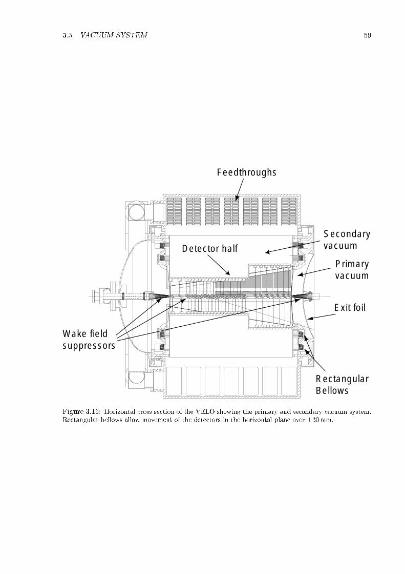
3.5. VACUUM SYSTEM 59
Feedthroughs
Detector half
Secondaryvacuum
Primaryvacuum
Exit foil
RectangularBellows
Wake fieldsuppressors
Figure 3.16: Horizontal cross section of the VELO showing the primary and secondary vacuum system.Rectangular bellows allow movement of the detectors in the horizontal plane over 30mm.
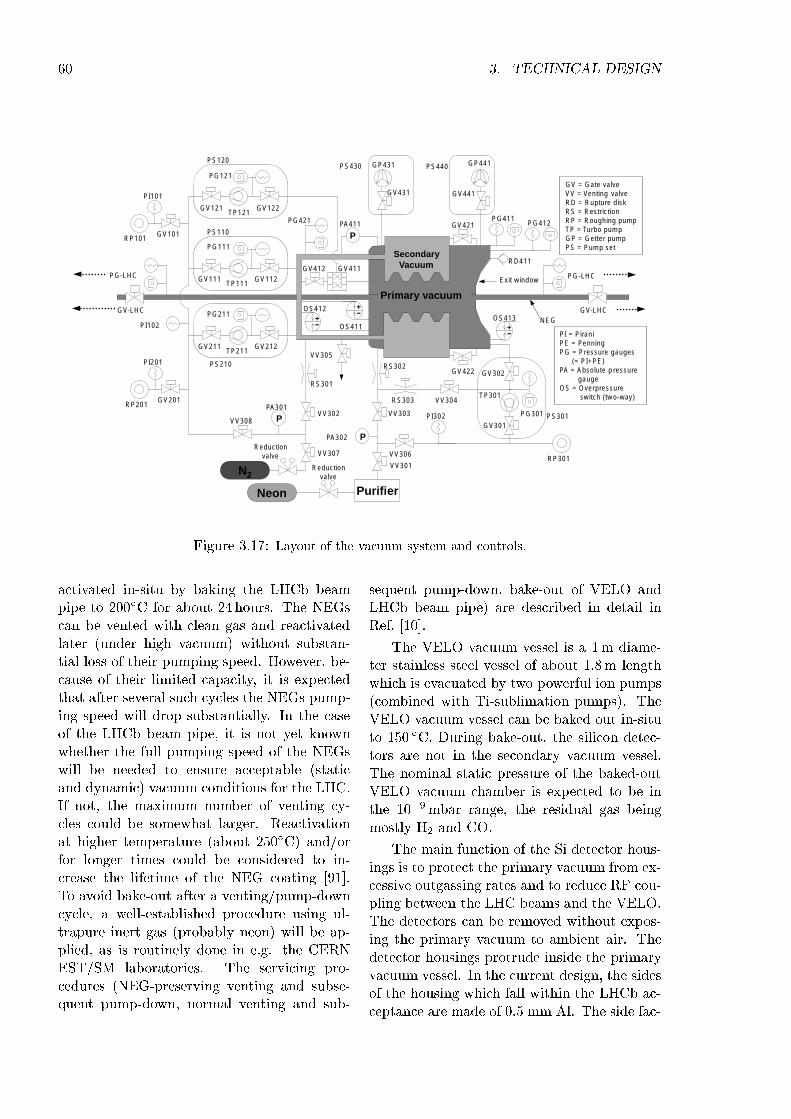
60 3. TECHNICAL DESIGN
PS120
PS110
PS210
GV121 GV122TP121
PG121
GV111 GV112TP111
PG111
GV211 GV212TP211
PG211
RP101
RP201GV201
GV101
PI201
PI101
PG-LHC
GV-LHC
PI102
GV = Gate valveVV = Venting valveRD = Rupture diskRS = RestrictionRP = Roughing pumpTP = Turbo pumpGP = Getter pumpPS = Pump set
PG421
GV412RD411
GP431
GV431
PS430 GP441
GV441
PS440
PA411PG411
PG412
PG-LHC
PI = PiraniPE = PenningPG = Pressure gauges (= PI+PE)PA = Absolute pressure gaugeOS = Overpressure switch (two-way)
GV-LHCOS412
OS411
Reductionvalve
VV301
PA301
VV306
PG301
GV302
TP301
GV301
RP301
PI302VV302 VV303
VV304
VV305
RS302
RS303
RS301
PS301
Reductionvalve
NEG
Exit window
VV308
VV307
OS413
PA302
GV411
PurifierNeon
-+-+
P
SecondaryVacuum
N2
P
P
-+
Primary vacuum
GV421
GV422
Figure 3.17: Layout of the vacuum system and controls.
activated in-situ by baking the LHCb beampipe to 200ÆC for about 24 hours. The NEGscan be vented with clean gas and reactivatedlater (under high vacuum) without substan-tial loss of their pumping speed. However, be-cause of their limited capacity, it is expectedthat after several such cycles the NEGs pump-ing speed will drop substantially. In the caseof the LHCb beam pipe, it is not yet knownwhether the full pumping speed of the NEGswill be needed to ensure acceptable (staticand dynamic) vacuum conditions for the LHC.If not, the maximum number of venting cy-cles could be somewhat larger. Reactivationat higher temperature (about 250ÆC) and/orfor longer times could be considered to in-crease the lifetime of the NEG coating [91].To avoid bake-out after a venting/pump-downcycle, a well-established procedure using ul-trapure inert gas (probably neon) will be ap-plied, as is routinely done in e.g. the CERNEST/SM laboratories. The servicing pro-cedures (NEG-preserving venting and subse-quent pump-down, normal venting and sub-
sequent pump-down, bake-out of VELO andLHCb beam pipe) are described in detail inRef. [10].
The VELO vacuum vessel is a 1m diame-ter stainless steel vessel of about 1:8m lengthwhich is evacuated by two powerful ion pumps(combined with Ti-sublimation pumps). TheVELO vacuum vessel can be baked out in-situto 150 ÆC. During bake-out, the silicon detec-tors are not in the secondary vacuum vessel.The nominal static pressure of the baked-outVELO vacuum chamber is expected to be inthe 109mbar range, the residual gas beingmostly H2 and CO.
The main function of the Si detector hous-ings is to protect the primary vacuum from ex-cessive outgassing rates and to reduce RF cou-pling between the LHC beams and the VELO.The detectors can be removed without expos-ing the primary vacuum to ambient air. Thedetector housings protrude inside the primaryvacuum vessel. In the current design, the sidesof the housing which fall within the LHCb ac-ceptance are made of 0:5 mm Al. The side fac-
3.5. VACUUM SYSTEM 61
ing the beams is made of 0:25 mm Al. The twodetector housings are evacuated by two turbo-molecular pump stations.
The LHCb beam pipe, besides being a frag-ile vacuum structure, constitutes a sensitivepart of the high vacuum system because of theactive NEG coating. Several options are be-ing studied to ensure that the interior of theprimary vacuum system will be minimally ex-posed to ambient air during an access to pri-mary vacuum components. One of the options,for example, is to enclose the LHCb VELO andRICH1 sub-systems in a clean area with a con-trolled atmosphere (low humidity, dust-free).In any case, the VELO setup will be located ina closed and possibly restricted area for reduc-ing risk due to human action. Furthermore, allservicing and maintenance operations on theVELO setup will be performed exclusively byqualied personnel.
The complete vacuum system will be con-trolled by a PLC unit backed with an unin-terruptable power supply and interfaced to theLHC and LHCb SCADA systems (via e.g. eth-ernet). In addition to this software interface,hard-wired interlocks between LHC and LHCbwill be implemented, for example for operationof the sector valves.
3.5.2 Protection devices of the LHCbvacuum system
Two kinds of safety valves are used to pro-tect the thin separation foil (detector housing)from an irreversible deformation, or rupture,in case of a pressure increase on either side ofthe foil. A dierential pressure switch is usedto open an electrically activated valve when-ever the pressure dierence between the pri-mary and secondary vacua rises above a value' 1mbar. If the pressure dierence exceedsthe value ' 5mbar, then the gravity-controlledvalve (see section 2.5.3) opens under the di-rect eect of the pressure independently ofany electrical power or pressurized air supply.The purpose of these safety valves is to main-tain the pressure dierence below ' 17mbar,the value above which the thin-walled detec-
tor housing is expected to deform irreversibly.Note that, at this pressure, the largest (per-manent) displacement on the encapsulation isabout 0:3mm. The actual rupture pressureof the encapsulation is expected to be severalhundred mbar [89].
The eect of a leak in the LHCb vacuumsection on its neighboring sections should beminimized, and vice versa. The implemen-tation and impact of fast separation valvesbetween LHCb and its neighboring LHC sec-tions are under study. Furthermore, to protectthe LHC ring vacuum against possible human-induced mishaps, the sector valves aroundLHCb will be automatically closed wheneveraccess to the experimental area is granted.
The LHCb equipment will be divided intosubsystems, each having its own battery back-up (Uninterruptable Power Supply, UPS).These UPS's can take over instantly after apower failure. However, their autonomy timeis about 10 minutes. To protect against longerpower failures, LHCb will rely on a high-powerdiesel generator. Since the take-over time ofsuch a generator is of the order of one minute,the distributed UPS's are indispensable. Inthe case of the VELO, all PLC units, vacuumvalves and monitoring devices (gauges, tem-perature sensors, etc.) will be backed up byUPS. The vacuum pumps are not backed upby UPS, but can be powered up by the dieselgenerator.
3.5.3 LHCb vacuum: eects on LHCoperation
LHC constraints on the residual pressure inthe primary vacuum vessel are rather loose.For instance, a modest pressure of the orderof 107mbar (H2 at room temperature) wouldcontribute negligibly to the integrated densityover the LHC ring. More important are possi-ble beam-induced eects which result from thebombardment of the surfaces surrounding thebeams by photons, electrons or ions. Thesephenomena can result in a local `run-away' ofgas density or electron cloud density. Dynamicpressure eects have been simulated by the
62 3. TECHNICAL DESIGN
CERN LHC-VAC group [92] for a (now ob-solete) version of the VELO design which didnot allow for bake-out of the primary vacuumwalls. The model included ion- and photon-induced desorption, but no electron-induceddesorption. The latter contribution is expectedto be negligible (unless strong electron mul-tipacting eects take place). It was assumedthat the NEG coating in the LHCb beam pipedoes not contribute to the pumping speed andthat its desorption coeÆcients are as of an ac-tive NEG-coated surface. The pressure prolein the presence of the two beams was calcu-lated numerically for increasing beam current.The current at which the pressure diverges iscalled the critical current and is required to belarger than 3:4 A (220:85A, where the rstfactor of 2 is a safety factor, the second one isfor the two beams). A number of instructiveconclusions can be drawn from the results ofthese simulations, the main one being that byoptimizing the geometry of the detector encap-sulations (thereby increasing the linear pump-ing speed along the beam axis) it is possibleto raise the critical current above the requiredvalue.
On the basis of the above considerations,one does not expect ion- and photon-induceddesorption phenomena to be an obstacle tonormal LHC operation. Moreover, with thelatest design of the VELO (see section 3.4),which allows for baking out the primary vac-uum surfaces, ion- and photon-induced phe-nomena are expected to be negligible.
Preliminary studies have shown that elec-tron cloud build-upmay occur when the VELOis in the open position. The eects on thegas pressure may be tolerated due to the largepumping speed. However, the emittance in-crease due to electron space charge has yet tobe assessed. A coating with low secondaryelectron yield on the detector encapsulationmight be necessary.
3.5.4 Risk analysis
A risk analysis was carried out for the VELOto rst identify critical parts of the system
and their possible failure scenarios, then toestimate the associated damage (essentially,the downtime for LHC) and nally to denea number of requirements (tests and precau-tions) to be fullled in order to bring the sys-tem to a level of acceptability compatible withLHC standards. The detailed risk analysis isdiscussed in Ref. [15]. The main conclusionis that, even in the worst scenario (rupturingof the exit window or LHCb beam pipe), thedowntime for LHC is not expected to exceedtwo weeks.
3.6 Cooling
A cooling system must be provided that al-lows operating the silicon detectors at a tem-perature adjustable between 25Æ and +10ÆC,while the temperature of the electronic com-ponents should be kept below 40ÆC. The to-tal heat produced in the detector amounts to1:2 kW. Including blackbody radiation fromneighboring parts and a safety factor of 1:5,the required cooling capacity is about 2:5 kW.The cooling system must be radiation resistantand the amount of material around the detec-tor should be minimized in order to limit theundesired production of background. Further-more, due to the required high positioning ac-curacy of the detector, temperature gradientsshould be kept minimal.
A two-phase cooling system has been se-lected with CO2 as a cooling agent. Refriger-ant R744 (CO2) has excellent cooling proper-ties8. CO2 is widely used as a cooling agentin radiation environments. No free radicalsand toxic compounds are expected to be pro-duced in the high-radiation environment of theVELO and the formation of carbon is inhibitedby the high recombination rate. The pressuredrop over the cooling capillaries in the mixedphase, which depends on the volume ratio be-tween vapor and liquid, compares favorablyfor CO2. As a result, the dimensions of the
8For a review of dierent cooling agents, we referto the review of the Air-Conditioning and Refrigera-tion Technology Institute in Arlington, VA, USA; seeRef. [93].
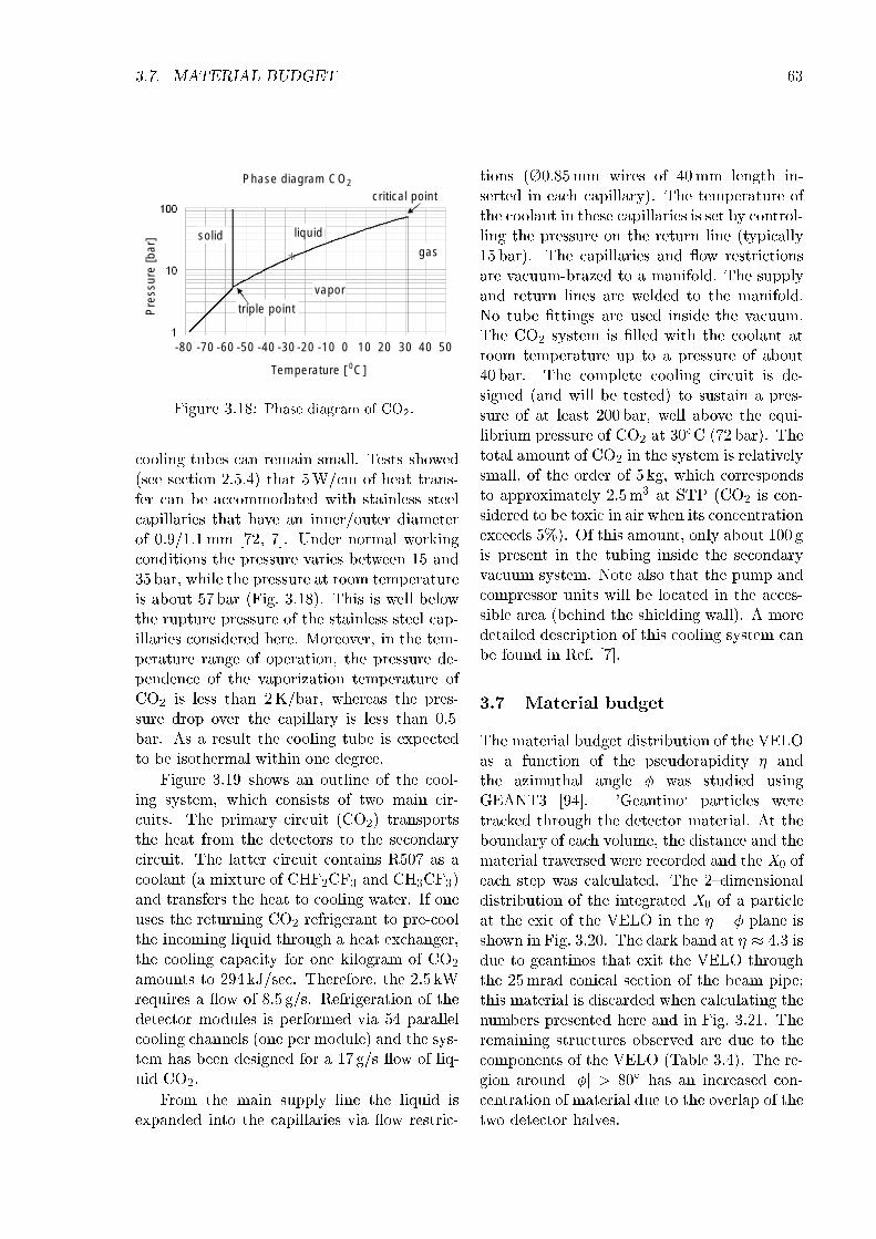
3.7. MATERIAL BUDGET 63
Phase diagram CO2
critical point
Pre
ssur
e [b
ar]
Temperature [ C]0
liquidsolid
vapor
triple point
gas
-80 -70 0 3020 4010-10-20-30-40-50-60 50
Figure 3.18: Phase diagram of CO2.
cooling tubes can remain small. Tests showed(see section 2.5.4) that 5W/cm of heat trans-fer can be accommodated with stainless steelcapillaries that have an inner/outer diameterof 0:9=1:1mm [72, 7]. Under normal workingconditions the pressure varies between 15 and35 bar, while the pressure at room temperatureis about 57 bar (Fig. 3.18). This is well belowthe rupture pressure of the stainless steel cap-illaries considered here. Moreover, in the tem-perature range of operation, the pressure de-pendence of the vaporization temperature ofCO2 is less than 2K/bar, whereas the pres-sure drop over the capillary is less than 0:5bar. As a result the cooling tube is expectedto be isothermal within one degree.
Figure 3.19 shows an outline of the cool-ing system, which consists of two main cir-cuits. The primary circuit (CO2) transportsthe heat from the detectors to the secondarycircuit. The latter circuit contains R507 as acoolant (a mixture of CHF2CF3 and CH3CF3)and transfers the heat to cooling water. If oneuses the returning CO2 refrigerant to pre-coolthe incoming liquid through a heat exchanger,the cooling capacity for one kilogram of CO2
amounts to 294 kJ/sec. Therefore, the 2:5 kWrequires a ow of 8:5 g/s. Refrigeration of thedetector modules is performed via 54 parallelcooling channels (one per module) and the sys-tem has been designed for a 17 g/s ow of liq-uid CO2.
From the main supply line the liquid isexpanded into the capillaries via ow restric-
tions (0:85mm wires of 40mm length in-serted in each capillary). The temperature ofthe coolant in these capillaries is set by control-ling the pressure on the return line (typically15 bar). The capillaries and ow restrictionsare vacuum-brazed to a manifold. The supplyand return lines are welded to the manifold.No tube ttings are used inside the vacuum.The CO2 system is lled with the coolant atroom temperature up to a pressure of about40 bar. The complete cooling circuit is de-signed (and will be tested) to sustain a pres-sure of at least 200 bar, well above the equi-librium pressure of CO2 at 30
ÆC (72 bar). Thetotal amount of CO2 in the system is relativelysmall, of the order of 5 kg, which correspondsto approximately 2:5m3 at STP (CO2 is con-sidered to be toxic in air when its concentrationexceeds 5%). Of this amount, only about 100 gis present in the tubing inside the secondaryvacuum system. Note also that the pump andcompressor units will be located in the acces-sible area (behind the shielding wall). A moredetailed description of this cooling system canbe found in Ref. [7].
3.7 Material budget
The material budget distribution of the VELOas a function of the pseudorapidity andthe azimuthal angle was studied usingGEANT3 [94]. 'Geantino` particles weretracked through the detector material. At theboundary of each volume, the distance and thematerial traversed were recorded and the X0 ofeach step was calculated. The 2dimensionaldistribution of the integrated X0 of a particleat the exit of the VELO in the plane isshown in Fig. 3.20. The dark band at 4:3 isdue to geantinos that exit the VELO throughthe 25mrad conical section of the beam pipe;this material is discarded when calculating thenumbers presented here and in Fig. 3.21. Theremaining structures observed are due to thecomponents of the VELO (Table 3.4). The re-gion around jj > 80Æ has an increased con-centration of material due to the overlap of thetwo detector halves.
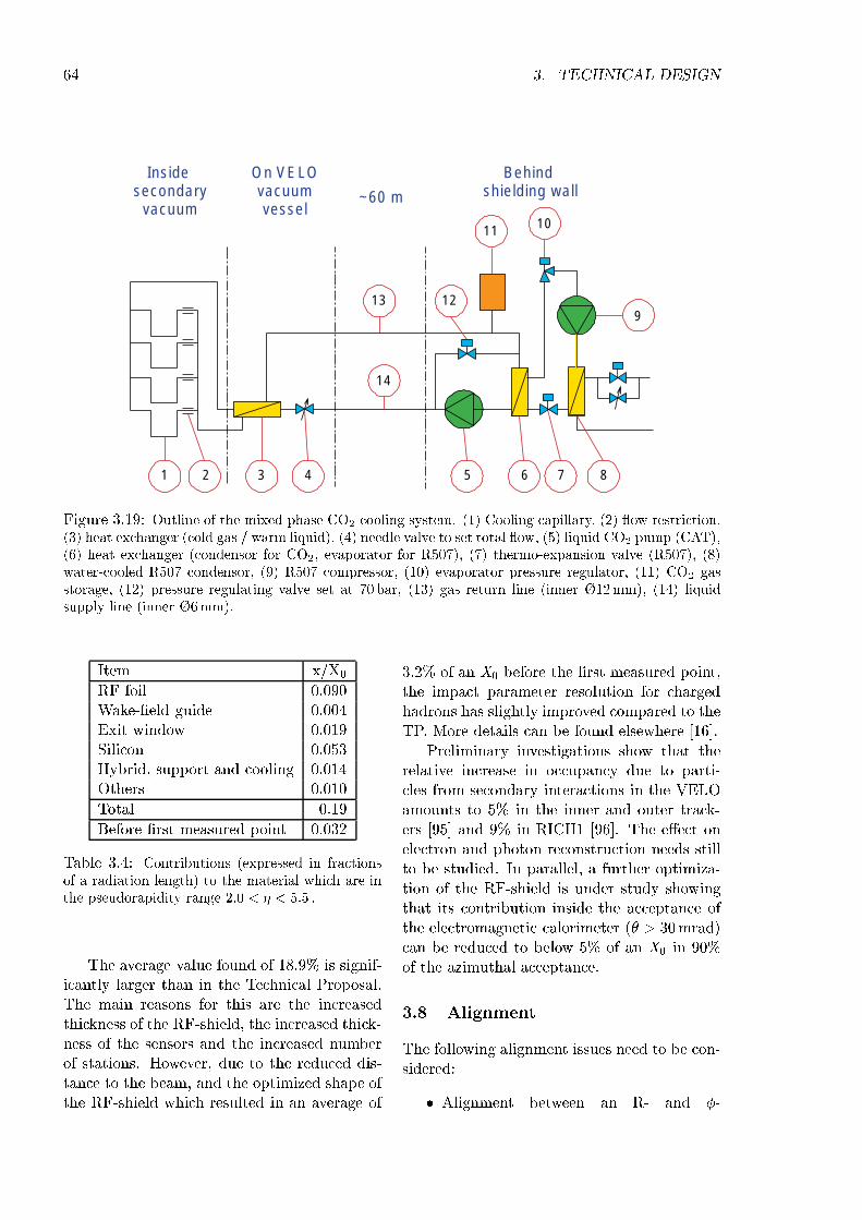
64 3. TECHNICAL DESIGN
Inside secondary
vacuum
On VELOvacuumvessel
Behind shielding wall~60 m
1 2 3 4 5 6 7 8
9
1011
1213
14
Figure 3.19: Outline of the mixed-phase CO2 cooling system. (1) Cooling capillary, (2) ow restriction,(3) heat exchanger (cold gas / warm liquid), (4) needle valve to set total ow, (5) liquid CO2 pump (CAT),(6) heat exchanger (condensor for CO2, evaporator for R507), (7) thermo-expansion valve (R507), (8)water-cooled R507 condensor, (9) R507 compressor, (10) evaporator pressure regulator, (11) CO2 gasstorage, (12) pressure regulating valve set at 70 bar, (13) gas return line (inner 12mm), (14) liquidsupply line (inner 6mm).
Item x=X0
RF foil 0.090Wake-eld guide 0.004Exit window 0.019Silicon 0.053Hybrid, support and cooling 0.014Others 0.010
Total 0.19
Before rst measured point 0.032
Table 3.4: Contributions (expressed in fractionsof a radiation length) to the material which are inthe pseudorapidity range 2:0 < < 5:5 .
The average value found of 18:9% is signif-icantly larger than in the Technical Proposal.The main reasons for this are the increasedthickness of the RF-shield, the increased thick-ness of the sensors and the increased numberof stations. However, due to the reduced dis-tance to the beam, and the optimized shape ofthe RF-shield which resulted in an average of
3:2% of an X0 before the rst measured point,the impact parameter resolution for chargedhadrons has slightly improved compared to theTP. More details can be found elsewhere [16].
Preliminary investigations show that therelative increase in occupancy due to parti-cles from secondary interactions in the VELOamounts to 5% in the inner and outer track-ers [95] and 9% in RICH1 [96]. The eect onelectron and photon reconstruction needs stillto be studied. In parallel, a further optimiza-tion of the RF-shield is under study showingthat its contribution inside the acceptance ofthe electromagnetic calorimeter ( > 30mrad)can be reduced to below 5% of an X0 in 90%of the azimuthal acceptance.
3.8 Alignment
The following alignment issues need to be con-sidered:
Alignment between an R- and -
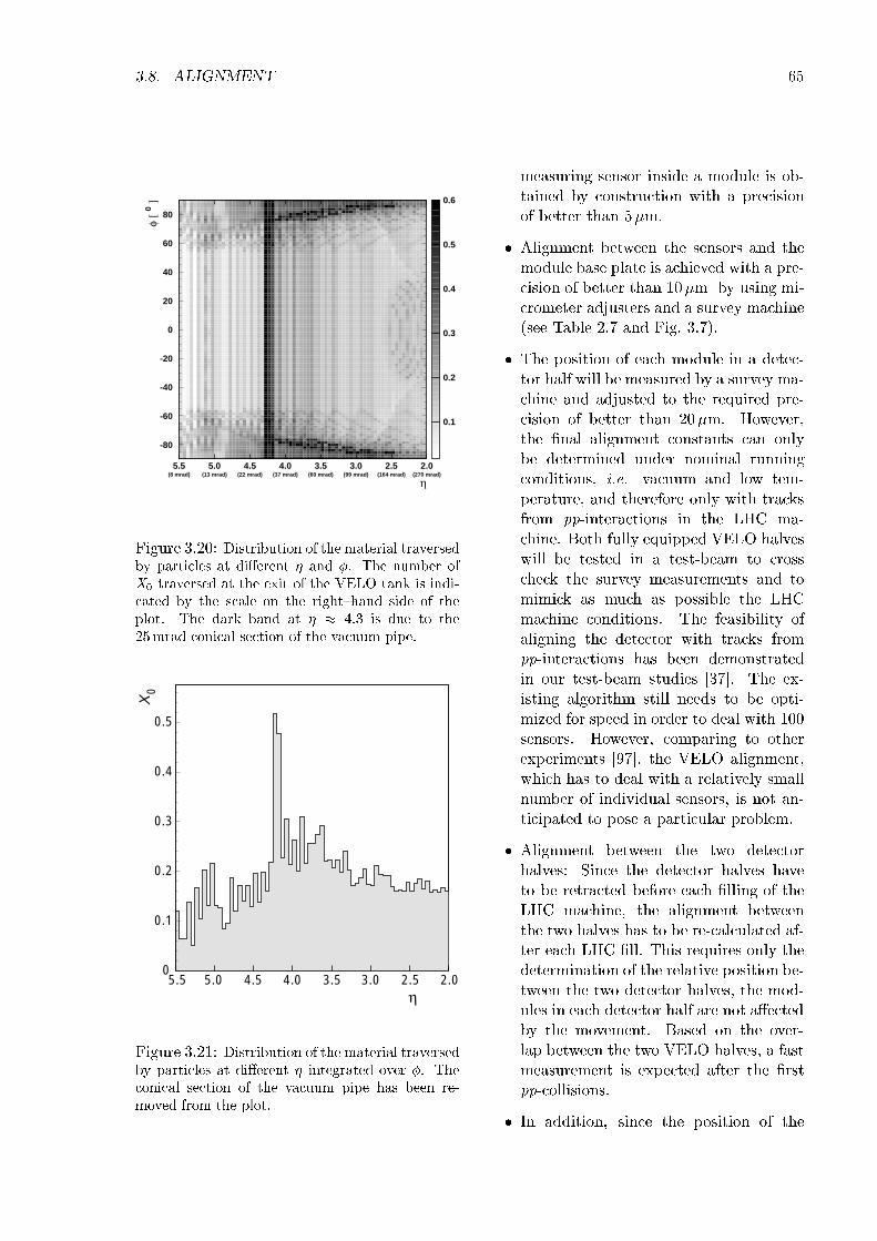
3.8. ALIGNMENT 65
0.1
0.2
0.3
0.4
0.5
0.6
(8 mrad) (13 mrad) (22 mrad) (37 mrad) (60 mrad) (99 mrad) (164 mrad) (270 mrad)
η
φ [ 0 ]
-80
-60
-40
-20
0
20
40
60
80
5.5 5.0 4.5 4.0 3.5 3.0 2.5 2.0
Figure 3.20: Distribution of the material traversedby particles at dierent and . The number ofX0 traversed at the exit of the VELO tank is indi-cated by the scale on the righthand side of theplot. The dark band at 4:3 is due to the25mrad conical section of the vacuum pipe.
η
X0
0
0.1
0.2
0.3
0.4
0.5
5.5 5.0 4.5 4.0 3.5 3.0 2.5 2.0
Figure 3.21: Distribution of the material traversedby particles at dierent integrated over . Theconical section of the vacuum pipe has been re-moved from the plot.
measuring sensor inside a module is ob-tained by construction with a precisionof better than 5m.
Alignment between the sensors and themodule base plate is achieved with a pre-cision of better than 10m by using mi-crometer adjusters and a survey machine(see Table 2.7 and Fig. 3.7).
The position of each module in a detec-tor half will be measured by a survey ma-chine and adjusted to the required pre-cision of better than 20m. However,the nal alignment constants can onlybe determined under nominal runningconditions, i.e. vacuum and low tem-perature, and therefore only with tracksfrom pp-interactions in the LHC ma-chine. Both fully equipped VELO halveswill be tested in a test-beam to crosscheck the survey measurements and tomimick as much as possible the LHCmachine conditions. The feasibility ofaligning the detector with tracks frompp-interactions has been demonstratedin our test-beam studies [37]. The ex-isting algorithm still needs to be opti-mized for speed in order to deal with 100sensors. However, comparing to otherexperiments [97], the VELO alignment,which has to deal with a relatively smallnumber of individual sensors, is not an-ticipated to pose a particular problem.
Alignment between the two detectorhalves: Since the detector halves haveto be retracted before each lling of theLHC machine, the alignment betweenthe two halves has to be re-calculated af-ter each LHC ll. This requires only thedetermination of the relative position be-tween the two detector halves, the mod-ules in each detector half are not aectedby the movement. Based on the over-lap between the two VELO halves, a fastmeasurement is expected after the rstpp-collisions.
In addition, since the position of the
66 3. TECHNICAL DESIGN
beam cannot be assured to be the samefor consecutive lls, its position needs tobe measured before moving the detectorsto their nal data-taking position. Withabout 100 minimum bias events, the dis-tance to the silicon stations can be mea-sured with 10m precision when the de-tectors are retracted by 3 cm from thebeam [98].
Alignment between the VELO and thedownstream detectors: The VELO willbe repositioned after each LHC lling op-erations with a precision of 50m whichis more precise then what is needed tolink the VELO tracks to the downstreamdetectors of LHCb.
3.9 Safety aspects
The Vertex Locator will comply with the safetypolicy at CERN (SAPOCO 42), and will followthe CERN safety rules and codes, the europeanand/or international construction codes whichare relevant for the detector construction andoperation. Possible specic risks, and actions,as discussed in the Initial Safety Discussion(ISD) with the Technical Inspection and Safety(TIS) Commission are summarized in the fol-lowing.
The two-phase CO2 cooling system willrun at a maximum pressure of 75 bar.The complete cooling circuit is designedand will be tested to sustain a pressureof up to 200 bar.
The temperature of the detector will bemonitored and in case of over tempera-ture, the electrical power of the detectorwill be switched o automatically.
Two powerful ion getter pumps will evac-uate the VELO vacuum chamber. Onlytrained personnel will be allowed to ma-nipulate this equipment9.
9ELECTRICAL SAFETY CODE C1.
The VELO vacuum vessel will be baked-out in-situ to 150 ÆC or more. A possibledamage to the detector is not consideredas a safety risk.
Any accessible metallic piece will beproperly grounded.
An initial study of induced radioactivityin the VELO vacuum vessel showed thatmaintenance work during shutdowns ispossible provided that proper precau-tions are taken [99].
The TIS commission concluded that nomajor safety problems were identied and pos-sible safety hazards will be excluded by proto-typing and testing the non standard equipmentincluding a high safety factor.
4 Simulation results
4.1 Software and event samples
The performance of the VELO system hasbeen studied using simulated data produced bythe oÆcial LHCb simulation and reconstruc-tion programs, SICBMC (v240) and SICBDST(v250) with database (v233). Proton-protoninteractions at
ps = 14TeV were simu-
lated using the PYTHIA (v6:1) event gener-ator [100]. A multiple-interaction model wasused, with varying impact parameter and run-ning pt cut-o, tuned [101] to reproduce exist-ing low-energy data. The LHCb apparatus wassimulated using GEANT3-based routines [94].The response of the silicon detectors was basedon a separate simulation, the results of whichwere veried with test-beam data [40].
The description of the VELO system in thesimulation followed as closely as possible thedesign given in this report, including the RF-shield, the wake eld guide, the cooling plates,the support frames and the parts of the vac-uum vessel which are in the LHCb acceptance.Further details can be found in [4, 102].
The following benchmark channels wereused to measure the performance of the VELO:minimum bias events, generic b-events andevents containing B0
d ! +, B0s ! Ds
+
and B0d ! J= K0
s () decays. The eventswere generated assuming a luminosity of 2 1032 cm2 s1. Each sample contained around30k events. The B-decays were selected withthe LHCb software package AXSEL [103] to re-strict the sample to events which can be recon-structed oine and contribute to the physicsanalysis.
4.2 Optimization
4.2.1 Overall detector optimization
During the process of optimizing the detectorlayout, many dierent designs were studied.The performance of each individual design wasjudged by analyzing the benchmark channels.Taking into account other constraints, such asthe necessary thickness of the RF-shield, theavailability of thin silicon detectors and thenite number of electronics channels, we de-cided on the design described in this document.Further improvements, for example reducingthe amount of material or using smaller strippitches, may become possible in the future.
4.2.2 Impact on L1 trigger
The L1 trigger is based on tracks with a sig-nicant impact parameter. Tracks are recon-structed based on VELO measurements aloneto minimize the amount of data which needsto be processed. As there is no magneticeld around the VELO, momentum informa-tion is in principle not available. Low momen-tum tracks can fake large impact parameters,i.e. signatures for tracks originating from B-decays, due to multiple scattering. In the algo-rithm employed for the L1 trigger as describedin the TP this contribution of fake tracks wasreduced by requiring track pairs to form sec-ondary vertices. It was found that increasingthe thickness of the RF-shield, from 100 m to250m, reduces the eÆciency of the L1 triggerin the B0
d ! +channel by 15%. Replacingthe corrugated RF-shield with a design whichresembles a beam pipe close to the beam-linewould reduce the L1 eÆciency by almost 30%.
To monitor the development of the VELO
67
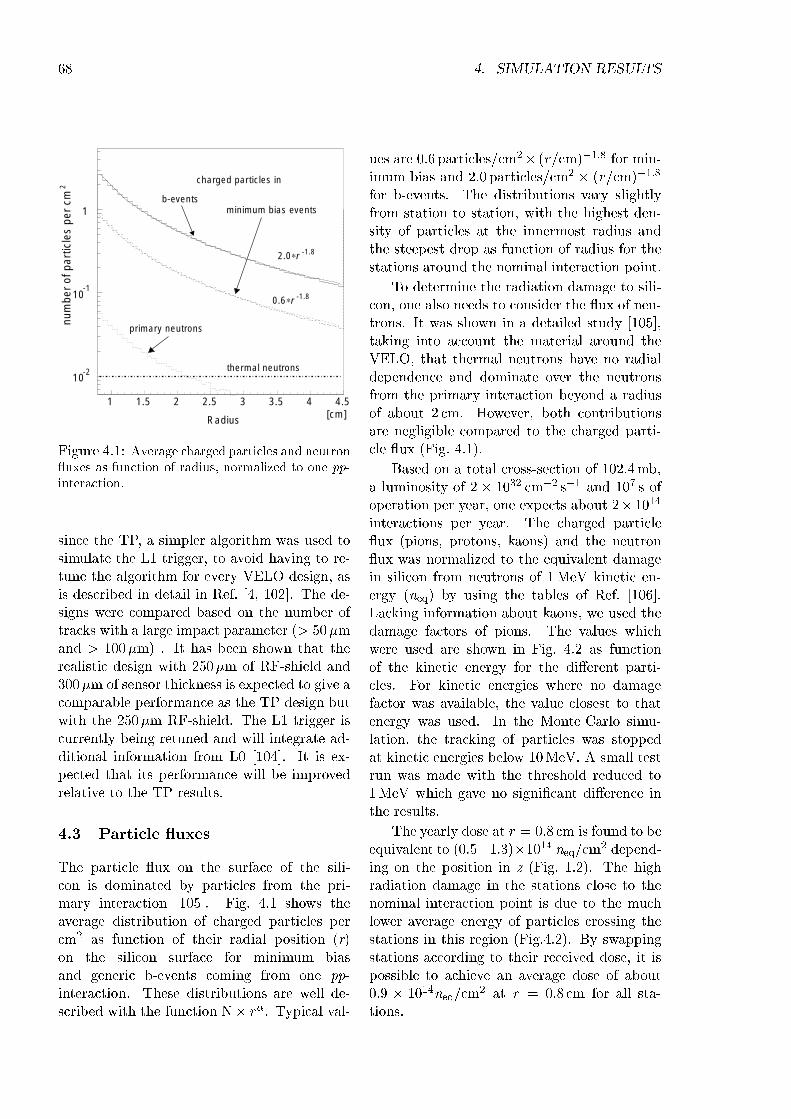
68 4. SIMULATION RESULTS
1 1.5 2 2.5 3 3.5 4 4.5[cm]
10-2
10-1
1
num
ber
of p
artic
les
per
cm2
b-eventsminimum bias events
thermal neutrons
primary neutrons
charged particles in
Radius
2.0∗r -1.8
0.6∗r -1.8
Figure 4.1: Average charged particles and neutron uxes as function of radius, normalized to one pp-interaction.
since the TP, a simpler algorithm was used tosimulate the L1 trigger, to avoid having to re-tune the algorithm for every VELO design, asis described in detail in Ref. [4, 102]. The de-signs were compared based on the number oftracks with a large impact parameter (> 50mand > 100m) . It has been shown that therealistic design with 250m of RF-shield and300m of sensor thickness is expected to give acomparable performance as the TP design butwith the 250m RF-shield. The L1 trigger iscurrently being retuned and will integrate ad-ditional information from L0 [104]. It is ex-pected that its performance will be improvedrelative to the TP results.
4.3 Particle uxes
The particle ux on the surface of the sili-con is dominated by particles from the pri-mary interaction [105]. Fig. 4.1 shows theaverage distribution of charged particles percm2 as function of their radial position (r)on the silicon surface for minimum biasand generic b-events coming from one pp-interaction. These distributions are well de-scribed with the function N r. Typical val-
ues are 0:6 particles=cm2 (r=cm)1:8 for min-imum bias and 2:0 particles=cm2 (r=cm)1:8
for b-events. The distributions vary slightlyfrom station to station, with the highest den-sity of particles at the innermost radius andthe steepest drop as function of radius for thestations around the nominal interaction point.
To determine the radiation damage to sili-con, one also needs to consider the ux of neu-trons. It was shown in a detailed study [105],taking into account the material around theVELO, that thermal neutrons have no radialdependence and dominate over the neutronsfrom the primary interaction beyond a radiusof about 2 cm. However, both contributionsare negligible compared to the charged parti-cle ux (Fig. 4.1).
Based on a total cross-section of 102:4mb,a luminosity of 2 1032 cm2 s1 and 107 s ofoperation per year, one expects about 2 1014
interactions per year. The charged particle ux (pions, protons, kaons) and the neutron ux was normalized to the equivalent damagein silicon from neutrons of 1MeV kinetic en-ergy (neq) by using the tables of Ref. [106].Lacking information about kaons, we used thedamage factors of pions. The values whichwere used are shown in Fig. 4.2 as functionof the kinetic energy for the dierent parti-cles. For kinetic energies where no damagefactor was available, the value closest to thatenergy was used. In the Monte Carlo simu-lation, the tracking of particles was stoppedat kinetic energies below 10MeV. A small testrun was made with the threshold reduced to1MeV which gave no signicant dierence inthe results.
The yearly dose at r = 0:8 cm is found to beequivalent to (0:51:3)1014 neq/cm2 depend-ing on the position in z (Fig. 1.2). The highradiation damage in the stations close to thenominal interaction point is due to the muchlower average energy of particles crossing thestations in this region (Fig.4.2). By swappingstations according to their received dose, it ispossible to achieve an average dose of about0:9 1014neq/cm
2 at r = 0:8 cm for all sta-tions.
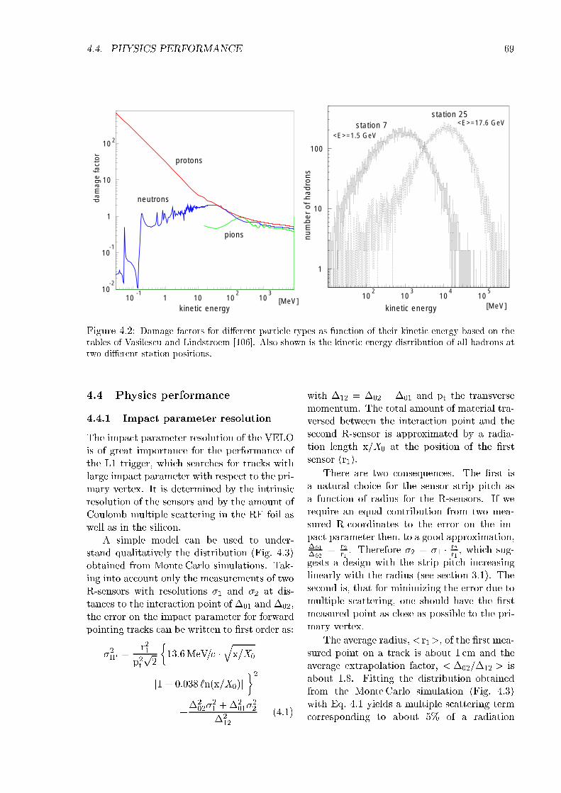
4.4. PHYSICS PERFORMANCE 69
10-2
10-1
1
10
102
10-1
1 10 102
103
[MeV]
dam
age
fact
or protons
neutrons
pions
kinetic energy
102
103
104
105
1
10
100
station 7station 25
kinetic energy [MeV]
<E>=17.6 GeV
<E>=1.5 GeV
num
ber
of h
adro
ns
Figure 4.2: Damage factors for dierent particle types as function of their kinetic energy based on thetables of Vasilescu and Lindstroem [106]. Also shown is the kinetic energy distribution of all hadrons attwo dierent station positions.
4.4 Physics performance
4.4.1 Impact parameter resolution
The impact parameter resolution of the VELOis of great importance for the performance ofthe L1 trigger, which searches for tracks withlarge impact parameter with respect to the pri-mary vertex. It is determined by the intrinsicresolution of the sensors and by the amount ofCoulomb multiple scattering in the RF foil aswell as in the silicon.
A simple model can be used to under-stand qualitatively the distribution (Fig. 4.3)obtained from Monte Carlo simulations. Tak-ing into account only the measurements of twoR-sensors with resolutions 1 and 2 at dis-tances to the interaction point of 01 and 02,the error on the impact parameter for forwardpointing tracks can be written to rst order as:
2IP =r21
p2tp2
13:6MeV=c
qx=X0
[1 + 0:038 `n(x=X0)]
2
+2
0221 +2
0122
212
(4.1)
with 12 = 02 01 and pt the transversemomentum. The total amount of material tra-versed between the interaction point and thesecond R-sensor is approximated by a radia-tion length x=X0 at the position of the rstsensor (r1).
There are two consequences. The rst isa natural choice for the sensor strip pitch asa function of radius for the R-sensors. If werequire an equal contribution from two mea-sured R-coordinates to the error on the im-pact parameter then, to a good approximation,01
02= r2
r1. Therefore 2 = 1 r2r1 , which sug-
gests a design with the strip pitch increasinglinearly with the radius (see section 3.1). Thesecond is, that for minimizing the error due tomultiple scattering, one should have the rstmeasured point as close as possible to the pri-mary vertex.
The average radius, <r1>, of the rst mea-sured point on a track is about 1 cm and theaverage extrapolation factor, < 02=12 > isabout 1:8. Fitting the distribution obtainedfrom the Monte Carlo simulation (Fig. 4.3)with Eq. 4.1 yields a multiple scattering termcorresponding to about 5% of a radiation
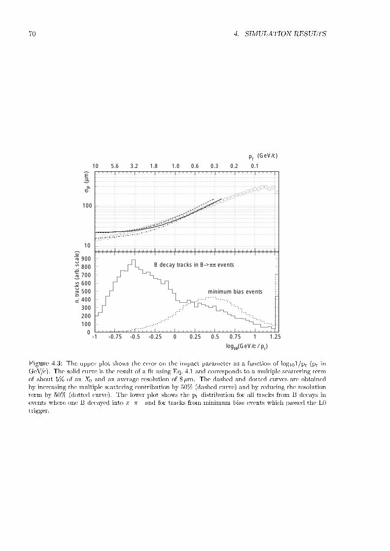
70 4. SIMULATION RESULTS
0100200300400500600700800900
-1 -0.75 -0.5 -0.25 0 0.25 0.5 0.75 1 1.25
n. tr
acks
(ar
b. s
cale
)
10 3.2 1.05.6 1.8 0.6 0.3
pT
(GeV/c)
10
100
σ IP (
µm)
log10(GeV/c / p )t
B decay tracks in B->ππ events
minimum bias events
0.2 0.1
Figure 4.3: The upper plot shows the error on the impact parameter as a function of log101=pt (pt inGeV=c). The solid curve is the result of a t using Eq. 4.1 and corresponds to a multiple scattering termof about 5% of an X0 and an average resolution of 8m. The dashed and dotted curves are obtainedby increasing the multiple scattering contribution by 50% (dashed curve) and by reducing the resolutionterm by 50% (dotted curve). The lower plot shows the pt distribution for all tracks from B decays inevents where one B decayed into + and for tracks from minimum bias events which passed the L0trigger.
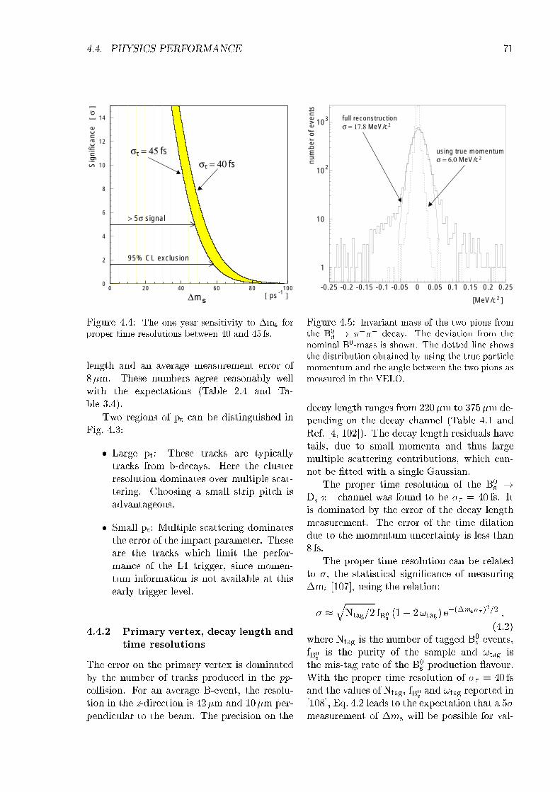
4.4. PHYSICS PERFORMANCE 71
0
2
4
6
8
10
12
14
0 20 40 60 80 100[ ps -1 ]
Sig
nific
ance
[ σ
]
> 5σ signal
95% CL exclusion
∆ms
σ = 45 fsτσ = 40 fsτ
Figure 4.4: The one year sensitivity to ms forproper time resolutions between 40 and 45 fs.
length and an average measurement error of8m. These numbers agree reasonably wellwith the expectations (Table 2.4 and Ta-ble 3.4).
Two regions of pt can be distinguished inFig. 4.3:
Large pt: These tracks are typicallytracks from b-decays. Here the clusterresolution dominates over multiple scat-tering. Choosing a small strip pitch isadvantageous.
Small pt: Multiple scattering dominatesthe error of the impact parameter. Theseare the tracks which limit the perfor-mance of the L1 trigger, since momen-tum information is not available at thisearly trigger level.
4.4.2 Primary vertex, decay length andtime resolutions
The error on the primary vertex is dominatedby the number of tracks produced in the pp-collision. For an average B-event, the resolu-tion in the z-direction is 42m and 10m per-pendicular to the beam. The precision on the
1
10
102
103
-0.25 -0.2 -0.15 -0.1 -0.05 0 0.05 0.1 0.15 0.2 0.25
[MeV/c ]nu
mbe
r of
eve
nts
2
full reconstructionσ = 17.8 MeV/c2
using true momentumσ = 6.0 MeV/c2
Figure 4.5: Invariant mass of the two pions fromthe B0
d ! + decay. The deviation from thenominal B0-mass is shown. The dotted line showsthe distribution obtained by using the true particlemomentum and the angle between the two pions asmeasured in the VELO.
decay length ranges from 220m to 375m de-pending on the decay channel (Table 4.1 andRef. [4, 102]). The decay length residuals havetails, due to small momenta and thus largemultiple scattering contributions, which can-not be tted with a single Gaussian.
The proper time resolution of the B0s !
Ds + channel was found to be = 40 fs. It
is dominated by the error of the decay lengthmeasurement. The error of the time dilationdue to the momentum uncertainty is less than8 fs.
The proper time resolution can be relatedto , the statistical signicance of measuringms [107], using the relation:
qNtag=2 fB0
s(1 2!tag) e
(ms )2=2 ;
(4.2)where Ntag is the number of tagged B0
s events,fB0
sis the purity of the sample and !tag is
the mis-tag rate of the B0s production avour.
With the proper time resolution of = 40 fsand the values of Ntag, fB0
sand !tag reported in
[108], Eq. 4.2 leads to the expectation that a 5measurement of ms will be possible for val-
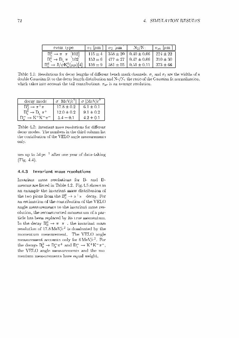
72 4. SIMULATION RESULTS
event type 1 [m ] 2 [m ] N2=N1 av [m ]
B0d ! +[102] 115 4 358 20 0:40 0:06 224 22
B0s ! Ds
+[102] 153 6 477 27 0:47 0:06 310 30B0d ! J= K0
s ()[4] 159 9 581 55 0:51 0:11 373 66
Table 4.1: Resolutions for decay lengths of dierent bench mark channels. 1 and 2 are the widths of adouble Gaussian t to the decay length distribution and N2=N1 the ratio of the Gaussian t normalization,which takes into account the tail contributions. av is an average resolution.
decay mode [MeV=c2] [MeV=c2]
B0d ! + 17:8 0:2 6:1 0:1
B0s ! Ds
+ 12:0 0:2 9:1 0:2Ds ! K+K 5:4 0:1 4:2 0:1
Table 4.2: Invariant mass resolutions for dierentdecay modes. The numbers in the third column listthe contribution of the VELO angle measurementsonly.
ues up to 54 ps1 after one year of data-taking(Fig. 4.4).
4.4.3 Invariant mass resolutions
Invariant mass resolutions for B- and D-mesons are listed in Table 4.2. Fig.4.5 shows asan example the invariant mass distribution ofthe two pions from the B0
d ! + decay. Foran estimation of the contribution of the VELOangle measurements to the invariant mass res-olution, the reconstructed momentum of a par-ticle has been replaced by its true momentum.In the decay B0
d ! +, the invariant massresolution of 17:8MeV=c2 is dominated by themomentum measurement. The VELO anglemeasurement accounts only for 6MeV=c2. Forthe decays B0
s ! Ds + and Ds ! K+K,
the VELO angle measurements and the mo-mentum measurements have equal weight.
5 Project organization
5.1 Schedule
The overall work programme and schedule issummarized in Fig. 5.1. It covers the periodup to spring 2006, when the rst LHC pilotrun is expected. The schedule is planned toensure that the VELO is installed and opera-tional before the beam starts. The period ofsingle beam in LHC is used for commissioningthe VELO in situ.
5.1.1 Completion of design and proto-typing
A realistic design of the VELO was describedin the previous chapter. Several of the tasksin the schedule require the evaluation of nalprototypes before the production can start.
1. Silicon: Sensors from dierent vendorsneed to be characterized. Some improve-ments can be achieved with additionalR&D, e.g. ultimate -sensor design with oating strips and thin n-on-n sensors.The prototyping of sensors will be com-pleted by a design review in the summerof 2002.
2. Front-end chip: The nal version of theSCTA VELO chip and a full workingBeetle chip are expected to arrive beforethe summer of 2001. Characterization ofthe two chips before and after irradiationwill be done before the end of 2001. Areview of the two chip options will takeplace in the beginning of 2002 and willlead to a decision which chip to use forthe rst VELO sensors.
3. Readout electronics: Prototypes of the16-chip hybrid, repeater electronics and
the L1 readout board will be producedand tested during 2001. The analoglink over 60m twisted pair cables will betested in a large scale system before theend of 2001.
4. Mechanics & Vacuum: The VELO un-derwent a conceptual design review [109]in April 2001. Further prototyping isneeded to characterize several compo-nents of the design. A production readi-ness review is foreseen for February 2002.
5. Alignment, monitoring and control: dif-ferent options are proposed to fulll thevarious tasks in this category, and proto-typing and testing will continue duringthe next test-beam runs.
5.1.2 Construction
The major construction tasks include:
1. Vacuum vessel: The whole system will bemanufactured at NIKHEF, including thesecondary/primary vacuum system, thedetector mounting system and the cool-ing system except of the thin exit window(LHC-VAC group). The progress will bereviewed on a yearly basis together withthe LHC machine groups involved. Com-pletion is foreseen during 2004.
2. Sensors: From past experience, abouthalf a year is needed to produce the sen-sors. The production of the front-endchips and the hybrids can partially pro-ceed in parallel. The construction of onecomplete detector module is expected totake about one week. This includes the
73
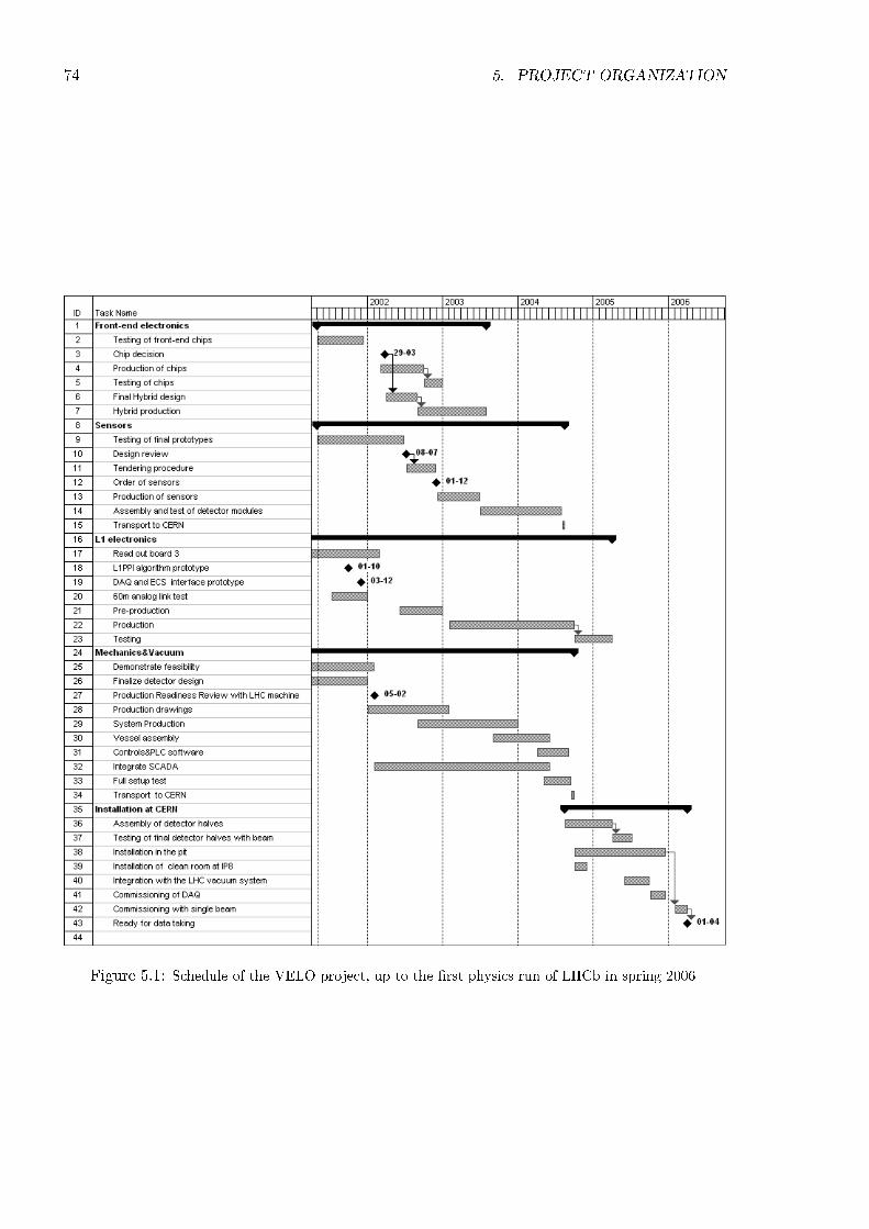
74 5. PROJECT ORGANIZATION
Figure 5.1: Schedule of the VELO project, up to the rst physics run of LHCb in spring 2006
5.2. MILESTONES 75
precise alignment of the sensors inside amodule. Several modules can be built inparallel.
3. Readout electronics: the front-end chipproduction is scheduled for the summerof 2002, in order to have the chips readyand tested for the module construction.Production of the readout electronicschain (from vacuum vessel pin-out toDAQ) is scheduled to be completed bythe end of 2004. These involve commonLHC developments (TTC chipset) andthe ECS interface. The L1 electronicsmake maximum use of FPGAs to imple-ment specic functionality. The modulesare situated in the counting room and arenot exposed to a high radiation dose.
4. Testing: systematic tests and certica-tion of the silicon sensors and readoutelectronics will be a time-consuming taskand must follow the production process.
It is planned to test the two detectorhalves in a charged particle beam duringthe rst half of 2005.
5.1.3 Installation and commissioning
Installation of the VELO vessel can start af-ter the LHC octant test in September 2004.A clean area at the interaction point needs tobe set-up to minimize the pollution of pieceswhich will be placed inside the primary or sec-ondary vacuum. The vacuum vessel will beconnected to the LHC vacuum control systemby autumn 2005.
The L1 electronics installation will start atthe begin of 2005. The system will be ready tostart commissioning of the DAQ with the otherLHCb sub-detectors in October 2005. Fivemonths of operation in this mode are foreseento ensure that the VELO is ready to take dataat nominal LHCb luminosity by April 2006.Valuable initial measurements concerning theRF shielding can be done during the LHC sin-gle beam operation before the rst pilot runwith collisions.
Cables Number Space (cm2)6400 analog links:twisted pair ND36P 400 960ECS: Cat5 1 0:25TTC: optical link 4 0:4HV power cables 100 25LV power cables 225 225PipesCO2 cooling 2 10
Table 5.1: List of dierent cables and space neededin the shielding wall.
The logistics of the VELO is situated at thefollowing positions:
The vacuum pumps are directly mountedonto the vacuum vessel.
The ECS transceiver boards are locatedclose to the VELO at a distance of about12m.
The L1 electronics and all the power sup-plies are situated behind the shieldingwall. At the same place, about 2m2 ofspace are needed for the compressor andthe pump units of the CO2-cooling sys-tem. The space needed for cables in theshielding wall is summarized in Table 5.1.If a packing of 60% is assumed, then thetotal space needed amounts to 0:2m2.
5.2 Milestones
Key milestones for the VELO project are listedin Table 5.2.
5.3 Costs
The total cost for the VELO is estimated tobe 4850 kCHF. The details are summarized inTable 5.3. Where appropriate, spares havebeen included. Most of the estimates are basedon quotes from industry or recent purchasesof similar items (e.g. prototype detectors,feedthroughs).
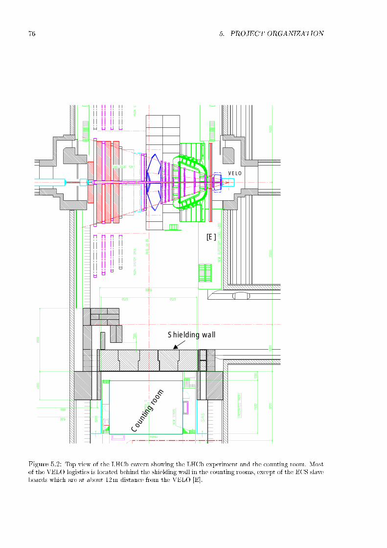
76 5. PROJECT ORGANIZATION
Shielding wall
Cou
ntin
g ro
om
[E]
VELO
Figure 5.2: Top view of the LHCb cavern showing the LHCb experiment and the counting room. Mostof the VELO logistics is located behind the shielding wall in the counting rooms, except of the ECS slaveboards which are at about 12m distance from the VELO [E].
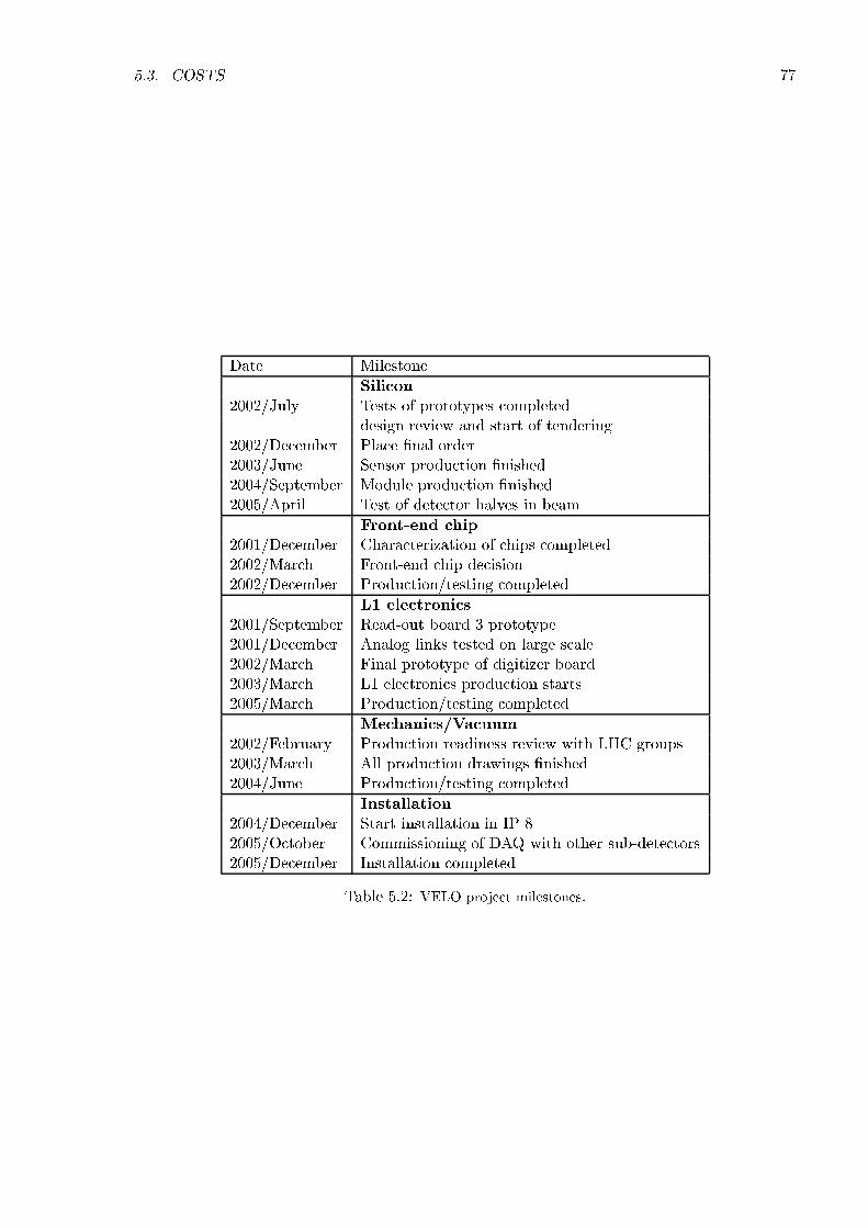
5.3. COSTS 77
Date Milestone
Silicon2002/July Tests of prototypes completed
design review and start of tendering2002/December Place nal order2003/June Sensor production nished2004/September Module production nished2005/April Test of detector halves in beam
Front-end chip2001/December Characterization of chips completed2002/March Front-end chip decision2002/December Production/testing completed
L1 electronics2001/September Read-out board 3 prototype2001/December Analog links tested on large scale2002/March Final prototype of digitizer board2003/March L1 electronics production starts2005/March Production/testing completed
Mechanics/Vacuum2002/February Production readiness review with LHC groups2003/March All production drawings nished2004/June Production/testing completed
Installation2004/December Start installation in IP 82005/October Commissioning of DAQ with other sub-detectors2005/December Installation completed
Table 5.2: VELO project milestones.
78 5. PROJECT ORGANIZATION
Item Number sub-totalof units (kCHF)
Mechanics&Vacuum: 1407Vacuum Vessel 1Vacuum equipmentCooling systemPatch panels 4Feedthrough anges1 28Secondary vacuum container 2Wake eld suppressorsTi evaporatorsPositioning mechanismCables and connectorsMonitoring and control
Silicon detectors: 635Sensors 125Hybrid 125
Electronics: 2780Frontend chips 1600Digitizer boards including analog data links 100TTC & ECS interface 100Data links to Readout Unit 100Readout Units 25Data links to L1 trigger 100Readout Units for L1 trigger 20LV1 interface 100DAQ interface 100Crates 5High voltage power supplies 100Low voltage power supplies 100
TOTAL 4822
Table 5.3: VELO project costs (kCHF). 1includes feed-throughs for pile-up VET0.
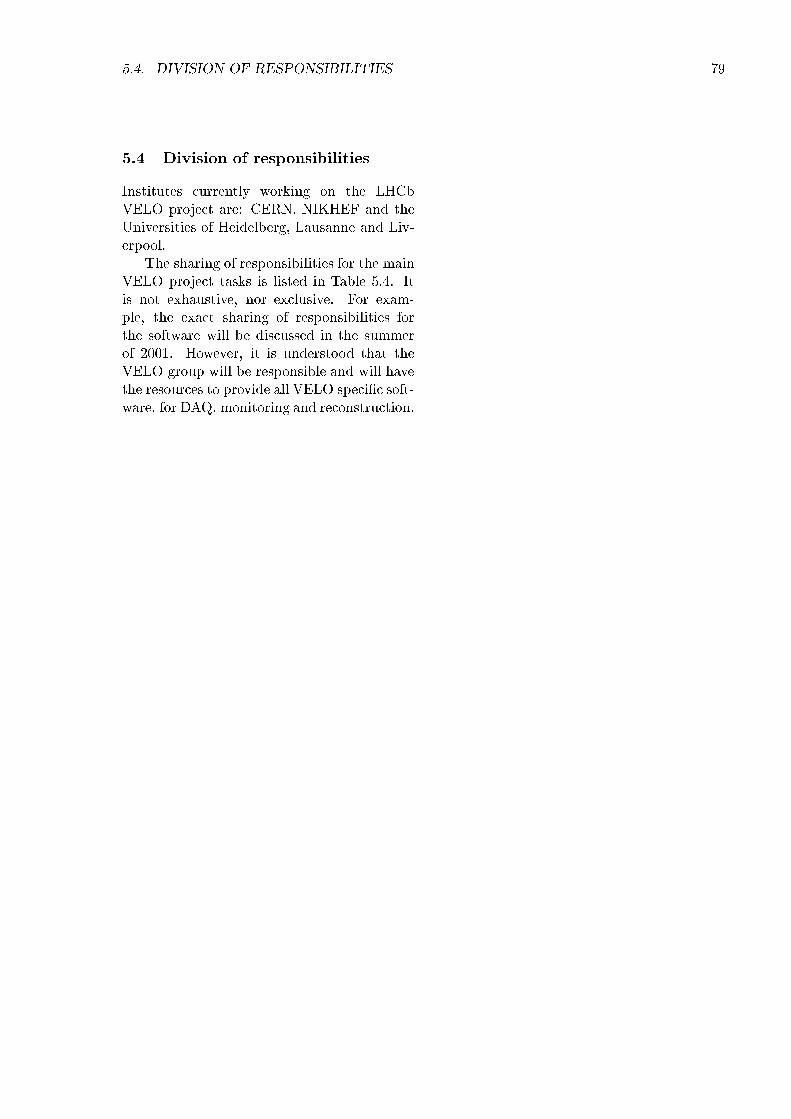
5.4. DIVISION OF RESPONSIBILITIES 79
5.4 Division of responsibilities
Institutes currently working on the LHCbVELO project are: CERN, NIKHEF and theUniversities of Heidelberg, Lausanne and Liv-erpool.
The sharing of responsibilities for the mainVELO project tasks is listed in Table 5.4. Itis not exhaustive, nor exclusive. For exam-ple, the exact sharing of responsibilities forthe software will be discussed in the summerof 2001. However, it is understood that theVELO group will be responsible and will havethe resources to provide all VELO specic soft-ware, for DAQ, monitoring and reconstruction.
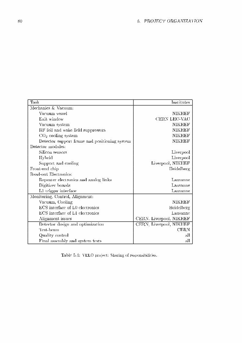
80 5. PROJECT ORGANIZATION
Task Institutes
Mechanics & Vacuum:Vacuum vessel NIKHEFExit window CERN LHC-VACVacuum system NIKHEFRF foil and wake eld suppressors NIKHEFCO2 cooling system NIKHEFDetector support frame and positioning system NIKHEF
Detector modules:Silicon sensors LiverpoolHybrid LiverpoolSupport and cooling Liverpool, NIKHEF
Front-end chip HeidelbergRead-out Electronics:
Repeater electronics and analog links LausanneDigitizer boards LausanneL1 trigger interface Lausanne
Monitoring, Control, Alignment:Vacuum, Cooling NIKHEFECS interface of L0 electronics HeidelbergECS interface of L1 electronics LausanneAlignment issues CERN, Liverpool, NIKHEF
Detector design and optimization CERN, Liverpool, NIKHEFTest-beam CERNQuality control allFinal assembly and system tests all
Table 5.4: VELO project: Sharing of responsibilities.
REFERENCES 81
References
[1] LHCb Technical Proposal, CERN/LHCC98-4.
[2] LHCb Magnet Technical Design Re-port, CERN/LHCC 2000-7; LHCbCalorimeters Technical Design Report,CERN/LHCC 2000-0036; LHCb RICHTechnical Design Report, CERN/LHCC2000-0037; LHCb Muon System TechnicalDesign Report, CERN/LHCC 2001-011.
[3] Study of the LHCb pile-up trigger and theBs ! J= decay, N. Zaitsev, PhD. The-sis, University of Amsterdam, 27 October2000.
[4] VELO Geometry Optimization, T. Bow-cock et al., LHCb 2000-090.
[5] Requirements for the L0 front-end elec-tronics, J. Christiansen, LHCb-99-029.
[6] Comparison of analogue and binary read-out in the silicon strips vertex detector ofLHCb, P. Koppenburg, LHCb-97-020.
[7] The CO2 cooling system for the LHCb ver-tex detector, H. Boer Rookhuizen et al.,LHCb-note, to be published.
[8] Mechanical Design of LHCb Vertex Loca-tor, LHCb 2001-083.
[9] C. Benvenuti et al., Vacuum 53 (1999)219-225.
[10] Conceptual design of the LHCb VELOvacuum system, J.F.J. van den Brand etal., LHCb 2001-080.
[11] A rst study of wake elds in the LHCbvertex detector, N. van Bakel et al., LHCb99-041.
[12] Wake elds in the LHCb vertex detector:strip shielding, N. van Bakel et al., LHCb99-043.
[13] Wake elds in the LHCb vertex detector:alternative designs for the wake eld sup-pressor, N. van Bakel et al., LHCb 99-044.
[14] Numerical calculation of the VELO cou-pling impedance, N. van Bakel et al.,LHCb 2001-082.
[15] Preliminary Risk Analysis for the LHCbVertex Detector, J.F.J. van den Brand etal., LHCb 2001-079.
[16] Material Distribution in the VELO,J. Libby, T. Ruf, M. McCubbin, LHCb-2001-019.
[17] Simulation of the vertex trigger preproces-sor: eects of noise on L1 performance,P. Koppenburg, LHCb-99-003.
[18] Overview of silicon detectors, H. Dijk-stra, http://lhcb-doc.web.cern.ch/lhcb-
doc/presentations/conferencetalks/2001.htm
[19] Charge collection eÆciency and resolu-tion of an irradiated double-sided siliconmicrostrip detector operated at cryogenictemperatures, K. Borer et al., Nucl. Instr.and Meth. A440 (2000) 17.
[20] Simulation of charge collection and shar-ing in microstrip detectors, T.J. Brod-beck, A. Chilingarov, Nucl. Instr. andMeth. A395 (1997) 29; Charge collec-tion eÆciency in heavily irradiated silicondiodes, L. Beattie et al., Nucl. Instr. andMeth. A412 (1998) 238.
[21] Micro-discharge noise and radiationdamage of silicon microstrip sensors,T. Ohsugi et al., Nucl. Instr. and Meth.A383 (1996) 166.
[22] A comparison of the performance of irra-diated p-in-n and n-in-n silicon microstripdetectors read out with fast binary elec-tronics, P.P. Allport et al., Nucl. Instr.and Meth. A450 (2000) 297.
[23] Design optimization of radiation-hard,double-sided, double-metal, AC-coupledsilicon sensors, T. Ohsugi et al., Nucl. In-str. and Meth. A436 (1999) 272.
[24] R.H. Richter et al., Nucl. Instr. and Meth.A377 (1996) 412;
82 REFERENCES
IEEE Trans. Nucl. Sci., vol. 47, n. 4, Au-gust 2000.
[25] ROSE Contribution to the LEB Work-shop, M. Moll:http://rd48.web.cern.ch/RD48/
6th-workshop/6th-workshop.htm
[26] Improving the radiation hardness proper-ties of silicon detectors using oxygenatedn-type and p-type silicon, G. Casse,P.P. Allport and M. Hanlon, IEEE Trans.Nucl. Sci., vol. 47, no. 3, June 2000;A comparative study of oxygenated andnon-oxygenated Si pad diodes, minia-ture and large area microstrip detectors,G. Casse et al., presented at the 4th In-ternational Symposium on Developmentand Application of Semiconductor Track-ing Detectors, Hiroshima, March 22-252000, to be published in Nuclear Instru-ments and Methods in Physics Research.
[27] Charge collection eÆciency of irradiatedsilicon detectors operated at cryogenictemperatures, K. Borer et al., Nucl. Instr.and Meth. A440 (2000) 5.
[28] Operating conditions of the VELO silicon,T. Bowcock, LHCb 2001-069.
[29] Detector Geometry - Vertex Locator test-beam software description, C. Parkes,LHCb-2000-096
[30] A VLSI chip produced by Integrated De-tectors and Electronics AS (IDE AS),Gaustadalleen 21, N-0371, Oslo, Norway;VIKING, a CMOS low noise monolithic128 channel frontend for Si-strip detectorreadout , O. Toker et al., Nucl. Instr. andMeth. A340 (1994) 572.
[31] SCTA - a Rad-Hard BiCMOS AnalogueReadout ASIC for the ATLAS Semincon-ductor Tracker, F. Anghinol et al., IEEETrans. Nucl. Science Vol.44, No.3, June1997.
[32] Noise Evaluation and Improvement of theLAL-RAL Microplex Readout Chip for the
DELPHI Vertex Detector, P. Seller et al.,Nucl. Instr. and Meth. A348 (1994) 444.
[33] Study of vertex silicon detectors for LHCexperiments, Thesis, S. Saladino, (CERN-OPEN-99-374), 3 December 1999.
[34] Track Fit - Vertex Locator Test-BeamSoftware Description, C. Parkes, LHCb2001-038.
[35] Results on the DELPHI microvertexalignment from a precise 3-D mapping,A. Andreazza et al., Nucl. Instr. andMeth. A312 (1992) 431.
[36] MINUIT reference manual, CERN Pro-gram Library Long Writeup Y250.
[37] Alignment of the 1998 VELO Test BeamData, I. Tomalin, LHCb 99-032.
[38] The L1 vertex trigger algorithm and itsperformance, H. Dijkstra, T. Ruf, LHCb98-006.
[39] Study of the Vertex Trigger Performanceon Test-Beam Data, F. Teubert, LHCb99-030.
[40] VELO Telescope Resolution and EÆ-ciency Measurements, P. Bartalini et al.,LHCb 2000-099
[41] Study of Resolution of VELO Test-BeamTelescope, V. Wright et al., LHCb 2000-103.
[42] Measurement of the Irradiation Prole atthe PS Beam, J. Libby, T. Ruf, F. Teubertand G. Casse, LHCb 2001-020.
[43] Performance of an irradiated n-on-nHamamatsu prototype VELO detector,T. Bowcock et al., LHCb 2001-039.
[44] Performance of an irradiated p-on-n Mi-cron prototype VELO detector, T. Bow-cock et al., LHCb 2001-040.
[45] Characterisation of an inhomogeneouslyirradiated microstrip detector using a nespot infrared laser, G. Casse et al., LHCb2001-053.
REFERENCES 83
[46] LHCb VELO Module Design, T. Bowcock,J. Carrol and A. Muir, LHCb 2001-068.
[47] Simulation and Measurements of the ther-mal performance of a LHCb VELO proto-type module, T. Bowcock, J. Carrol andP. Sutclie, LHCb 2001-070.
[48] HELIX 128 - An Amplier and Read-out Chip for MSGCs and Silicon Mi-crostrip Detectors, M. Feuerstack et al.,HD-ASIC-18-0696;HELIX - A Readout Chip for the HERA-B Microstrip Detectors 2nd Workshopon Electronics for LHC Experiments,W. Fallot-Burghardt et al., Balatonfured,Hungary, 1996.
[49] Results of the Industrial Transfer ofDMILL, a Rad-Hard Mixed Analog-Digital Technology for High-Energy-Physics Applications, M. Dentan etal., Proceedings of the 3rd Workshopon Electronics for LHC Experiments,CERN/LHCC/97-60.
[50] R. Brenner et al., Nucl. Instr. and Meth.A339 (1994) 564.
[51] 3rd RD49 Status Report, Study ofRadiation Tolerance of ICs for LHC,CERN/LHCC/2000-003 (2000).G. Anelli et al., Total Dose Behav-ior of Submicron and Deep-SubmicronCMOS Technologies, Proceedings of the3rd Workshop on Electronics for LHC Ex-periments, CERN/LHCC/97-60.
[52] Total Dose and Single Event Eects(SEE) in a 0.25 m CMOS Technology,F. Faccio et al., CERN/LHCC/98-36(1998).
[53] The performance of the SCTA ASIC whenreading out irradiated and non-irradiatedVELO prototype detectors, M. Charles,J. Buytaert and J. Libby, LHCb 2001-041.
[54] The SCTA VELO Reference Manual,J. Buytaert, LHCb 2001-045.
[55] Characterization of the Beetle-1.0 FrontEnd Chip, D. Baumeister et al., LHCb2001-049.
[56] Investigation of Characteristics and Radi-ation Hardness of the BeetleCO10 Chip,N. van Bakel et al., LHCb 2001-037.
[57] Vertex Detector Electronics: ODE Pre-Prototype, User Manual Version 2.0,Y. Ermoline, IPHE note VELO 2000-008,LHCb 2001-057.
[58] TTCrx Reference Manual, V3.2, February2001, http://www.cern.ch/TTC/TTCrx manual3.2.pdf .
[59] Analog Device AD9059,http://www.analog.com/pdf/ad9059.pdf.
[60] Access Port and Boundary-ScanArchitecture (IEEE Std 1149.1)http://www.analog.com/pdf/ad9059.pdf
.
[61] LHCb VELO O Detector ElectronicsPreprocessor and Interface to the Level 1Trigger, A. Bay, G. Haefeli, P. Koppen-burg, LHCb 2001-043, IPHE 2000-019.
[62] Test of VELO detector FE chips usingthe ODE-PP, Y. Ermoline, G. Gagliardi,U. Parzefall, LHCb 2001-067, IPHE 2001-006.
[63] http://caenlab.caen.it/Catalogo.nsf/
(AllDoc)/V550V550A.
[64] Vertex Detector Electronics: RB3 Speci-cation Draft 4, Y. Ermoline, LHCb 2001-050, IPHE 2001-002.
[65] A Long Analog Transmission Line for theVELO Read-Out, R. Frei, G. Gagliardi,LHCb 2001-072 VELO, IPHE 2001-005.
[66] 40 Ms/s Analog transmission on shieldedtwisted pair cable J. Buytaert, LHCb-98-032.
[67] Shielding of the VELO detectors from theLHC beam high-frequency elds: prelimi-nary considerations, N. van Bakel et al.,LHCb 2001-081.
84 REFERENCES
[68] Y.H. Chin, User's Guide for ABCI Ver-
sion 8.7, CERN SL/94-02 (AP), see alsohttp://wwwinfo.cern.ch/parc/abci.
[69] LHCb Letter of Intent, CERN/LHCC 95-5, LHCC/I8, 25 August 1995.
[70] Single-Beam Collective Eects in theLHC, F. Ruggiero, LHC Note 313 (CERNSL/95-09 AP).
[71] see e.g. Coupling impedance measure-ments: an improved wire method, inV.G. Vaccaro INFN/TC-94/023, and J.G.Wang and S.Y. Zhang, Nucl. Instr. Meth.A459 (2001) 381.
[72] Design and test of a mixed-phase CO2
cooling system for the LHCb vertex detec-tor, O. Postma et al., LHCb 99-046.
[73] Radiation tests with foxfet biased mi-crostrip detectors R. Hammarstrom et al.,Nucl. Instr. and Meth. A418 (1998) 128.
[74] The DELPHI Silicon Tracker at LEP2P. Chochula et al., Nucl. Instr. and meth.A412 (1998) 304.
[75] The I2C-bus and how to use it, PhilipsSemiconductors, April 1995.
[76] Specications of the F/E-Chip for theLHCb Vertex Detector, M. Schmelling,LHCb 2001-048.
[77] Eect of Pulse Overspill on the Level 1Trigger, P. Koppenburg, LHCb 2001-078.
[78] The Beetle Reference Manual,D. Baumeister et al., LHCb 2001-046.
[79] SPAC: Serial Protocol for the AtlasCalorimeter, R. Bernier et al., 1998.
[80] The ECS Interface to the VELO Front-End Electronics, T. Glebe, LHCb 2001-044.
[81] A SPAC based solution for FEE-ECS,D. Breton, LHCb Electronics Workshop,Jan. 2001.
[82] Analog Device AD8055,http://www.analog.com/pdf/ad8055.pdf .
[83] Proceedings of the Beaune 97 Xth IEEEReal-Time Conference, H.C. van derBij et al., http://hsi.web.cern.ch/HSI/s-
link/introduc/rt97.ps .
[84] LHCb Level 1 Vertex Topology Trig-ger, Y. Ermoline, V. Lindenstruth andA. Walsch, LHCb Note 99-031.
[85] Subevent Transport Format (STF)for Readout Units and Link Multi-plexers, H. Muller and J. Toldeo,http://hmuller.home.cern.ch/hmuller/RU
/STFormat/stf.pdf .
[86] Mechanical and Vacuum Stability DesignCriteria for the LHC Experimental Vac-uum Chambers, I.R. Collins, O. Grobner,P. Lepeule, R. Veness, LHC Project Re-port 205.
[87] Aperture requirements around interactionIP8, G. von Holtey, LHCb note 97-002/EXPT.
[88] Design of the VELO exit window,J.R. Knaster et al., CERN LHC-VAC,Vacuum Technical Note to be published.
[89] http://www.nikhef.nl/pub/departments/-mt/projects/lhcb-vertex.
[90] Preliminary Studies for the LHCb VertexDetector Vacuum System, O. Postma etal., LHCb 99-045.
[91] C. Benvenuti et al., CERN EST/99-008(SM).
[92] LHCb Vacuum Calculations, A. Rossi etal., CERN LHC-VAC, Vacuum TechnicalNote to be published.
[93] ARTI, http://www.arti-21cr.org/db/dataarticle.pdf.
[94] CERN Program Library Long WriteupW5013 (1993).
REFERENCES 85
[95] The average occupancy in T2 and T3 in-creases by 5%, and does not change inT4 T11, Minutes of Tracking Meeting,March 27-28 2001 at NIKHEF.
[96] Relative increase in RICH 1: (9:0 0:6)%and RICH 2: (2:5 0:6)%, private com-munication J. Libby;A simulation study of the LHCb RICHperformance M. Adinol et al., LHCb2000-066 .
[97] Alignment of the DELPHI vertex detector,V. Chabaud, A. Andreazza, P. Collins,H. Dijkstra, DELPHI note 95177 MVX10, December 1995;Inner Tracking System, ALICE TDR 4,CERN/LHCC 99-12.
[98] The VELO as Beam Monitor, P. Jalocha,LHCb 2001-031.
[99] Induced radioactivity in the vacuumchamber, R. Wigmans, LHCb 2001-052.
[100] T. Sjostrand and M. Bengtsson, Comp.Phys. Comm. 43 (1987) 367.
[101] Tuning of Multiple Interactions Gener-ated by Pythia, P. Bartalini et al. LHCbnote 99-028.
[102] VELO Geometry Optimization - An Up-date, T. Bowcock et al., LHCb 2001-071.
[103] The AXSEL package, G. Corti, http://lhcb.cern.ch/ gcorti/analysis/axselect.html .
[104] The LHCb vertex locator and level-1 trig-ger, H. Dijkstra, LHCb 2000-001.
[105] Radiation environment at the LHCb ver-tex detector area, V. Talanov et al. LHCbnote 98-019.
[106] Displacement damage in silicon,on-line compilation, A. Vasilescu(INPE Bucharest) and G. Lind-stroem (University of Hamburg),http://sesam.desy.de/~gunnar/Si-dfuncs.html.
[107] Mathematical methods for B0B0oscilla-
tion analyses, H.-G. Moser, A. Roussarie,Nucl. Instr. and Meth. A384 (1997) 491.
[108] BDecays in `Proceedings of the work-shop in Standard Model Physics (andmore) at the LHC', P. Ball et al., CERN2000-04.
[109] LHCb Vertex Locator, ConceptualDesign Review, CERN/EST-LEA/2001-001/dl.


![90451 - TdR FLOTA DO IRIRI › ... › 90451---tdr-flota-do-iriri.pdfw p ] v ñ î ì $7,9,'$'(6 $ 6(5(0 '(6(192/9,'$6 (wdsdv wduhidv h uhvsrqvdelolgdghv $ h[hfxomr ghvwh whupr gh](https://static.fdocumentos.com/doc/165x107/60bbce7386e37e21a732e295/90451-tdr-flota-do-iriri-a-a-90451-tdr-flota-do-iriripdf-w-p-v-.jpg)